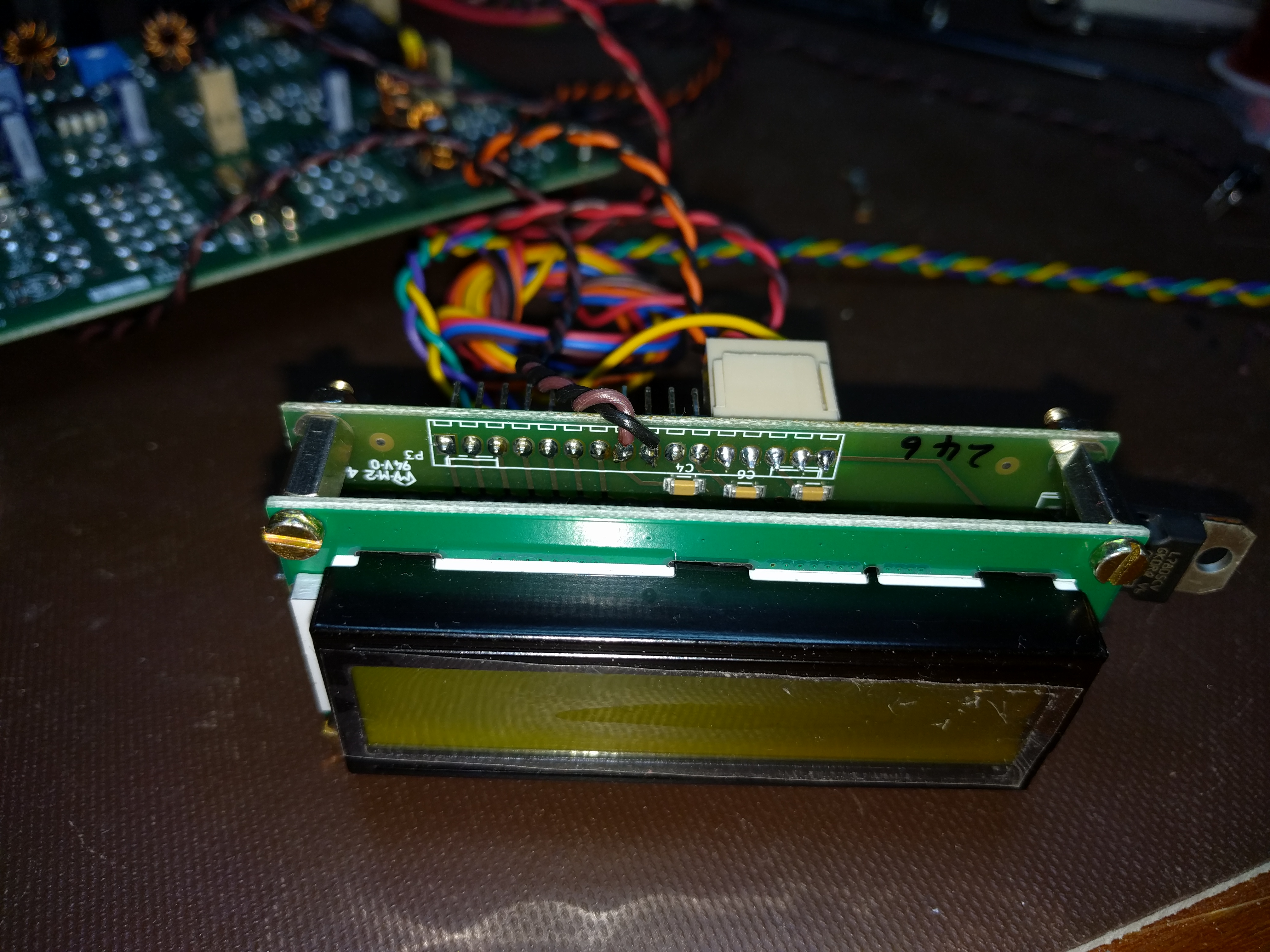
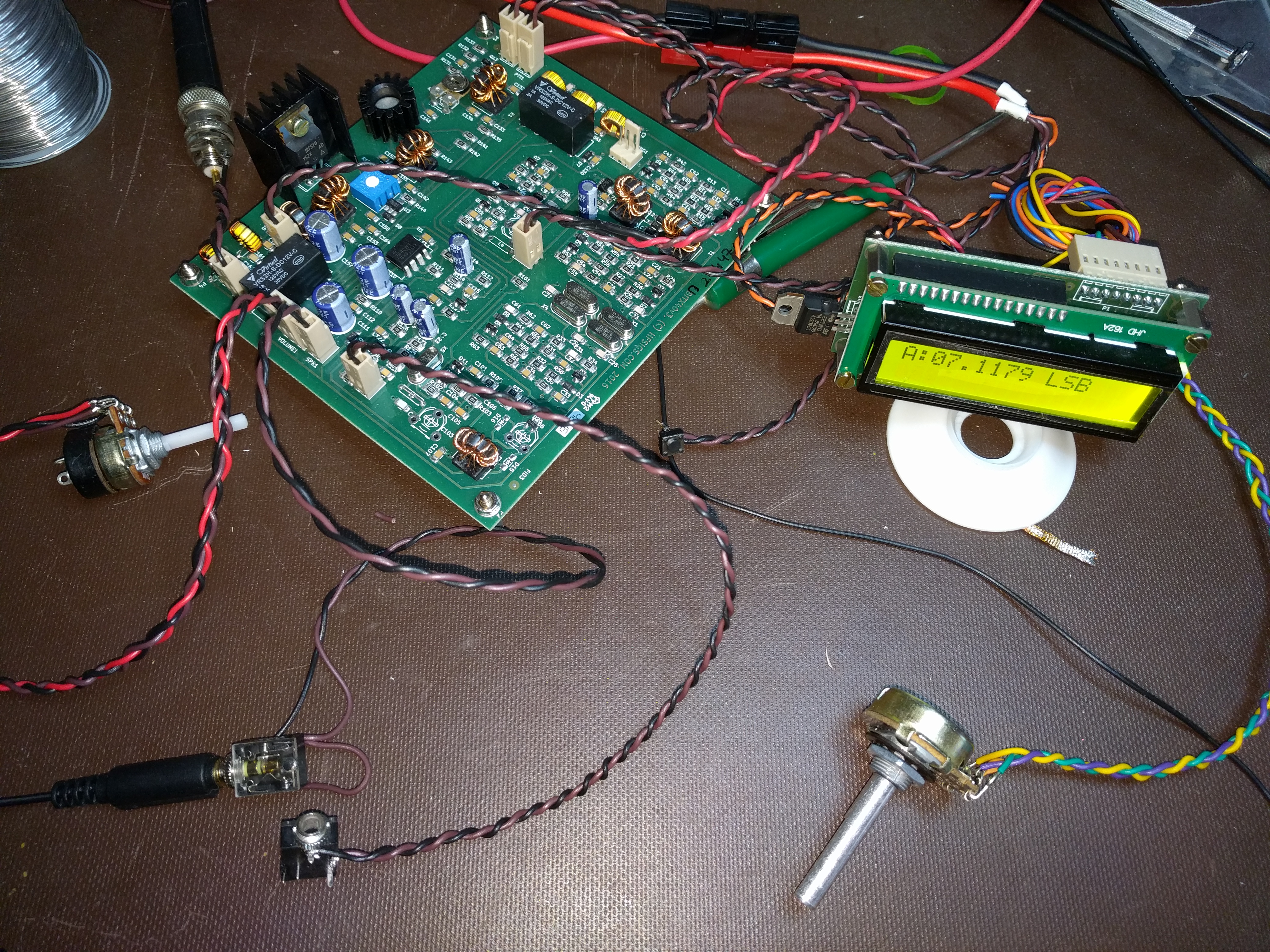
The BITX 40’s microphone amp has a flaw that may shorten the lifespan of microphones by overstressing their components. Here’s what I found and how I fixed it so far.
Here’s the BITX 40 mic amp schematic:

The mic bias is supplied by the TX line through 4.9K of resistance. TX is the DC power supply, 12-15V.
Most electret microphones have a maximum voltage of 10 V, though I’ve seen a few datasheets with a 9 V limit. The data sheets also say that the mics draw 0.5 mA maximum. No minimum is given.
Now, applying Ohm’s law,
 * (4.9 \mathrm{k\Omega}) = 2.45 \mathrm{V}")
Subtracting that from 12 V gives us 9.55 V, so one might think that everything is great.
Not really.
From the books of Bob Pease I learned the importance of worst case design. In worst case design, one looks at the datasheet minimum and maximum specifications and designs the circuit to work under the worst combination of specifications. Ignore the datasheet typical ratings, because those describe the best case. No one wants a circuit that only works in the best possible circumstances.
The BITX 40 docs specify a maximum power supply of 15 V, so that is the worst-case TX. The worst case microphone current is the minimum current, but I haven’t seen a mic datasheet that lists a minimum. Therefore, I have to make a guess. I need the guess to be on the safe side without being ridiculous. Knowing that the current is set by a JFET and knowing about both the variability of JFETs and how data sheet maximums are chosen, I could guess that the typical current is maybe half of the maximum and the minimum half of that, so 0.125 mA. If I want to make a truly robust circuit I could assume a minimum current of zero. I know a JFET can’t create current out of nothing, so the lowest possible current it draws is zero.
Let’s look at what voltages that creates:
 - (0.125 \mathrm{mA})(4.9 \mathrm{k\Omega}) = 14.388")
Uh-oh. That’s well above the 10 V maximum for the mic.
The zero current case is easier to work out. With zero current through the resistor, the mic sees the full 15 V.
A simple fix is to put a resistor in parallel with MIC1, making a voltage divider. I use a computer headset with my BITX, and I know that computer mics are typically fed with 5 V through a 2.2 kΩ resistor. Knowing that, I picked a 4.3 kΩ resistor across MIC1 to form a voltage divider equivalent to 2.3 kΩ fed by 7 V. That’s close enough, and 7 V is well below the maximum for most electret elements.
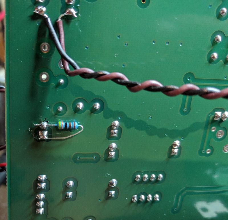
Unfortunately, the mic now drives an impedance about 30% lower than before, reducing its output. The RF drive, R136, should be adjusted to compensate.
One could fix the issue a different way, of course. A Zener diode in series with R121 could drop the voltage just as effectively without lowering the amplifier’s input impedance. An LM780x regulator could do the job, too, albeit with more components. I happened to have 1% resistors within reach and Zener diodes on a different floor of the house. I chose the resistor.
Is this a real problem?
No one else seems to have noticed this issue, so it’s worth asking whether it matters. One answer is that it is worthwhile, and pleasing, to do things right. There is a place for bodging a circuit together that works as a one-off, but I enjoy the n-dimensional puzzle of getting the details right.
The other answer is that it might be killing microphones, but not often enough that anyone has noticed. The BITX 20 mailing list, home to BITX 40 discussion, has seen a few comments from hams whose microphone capsules worked for a while, then failed. Some have been able to trace the problems to bad solder joints or physical damage, but I have to wonder if any of the remaining unsolved cases were caused by overvoltage.
Manufacturer maximum specifications are based on an assumption about the device’s expected lifetime. Operating beyond that specification can be expected to shorten the device’s lifetime. Sometimes that shortened lifetime is dramatic, with a flash of light, a puff of smoke, or an outpouring of heat. Other times it is subtle and takes longer. Perhaps mic elements will fail faster than usual. Perhaps their average lifespan will be 2 years instead of 20.
The difference might not be enough to notice, but we can fix it anyway. Worst case design will save the day.
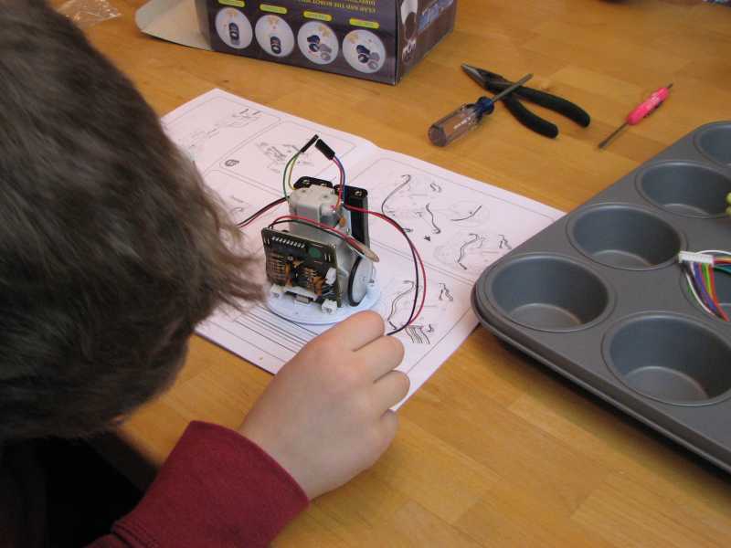
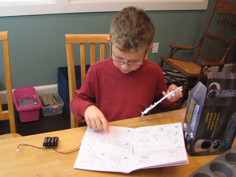 The kit is marketed for kids 13 and up. Nick is still in kindergarten, but loves anything motorized or electronic, so we did it together. The manual used exploded assembly diagrams to show how the pieces went together. Few words are used, and some skill in interpreting drawings is helpful in figuring out the steps. In other words, this was very much a collaborative effort for us. I figured out what went where, he found the parts, and we jointly did the assembly. Though one could probably do the project alone, there certainly were times when it helped to have four hands.
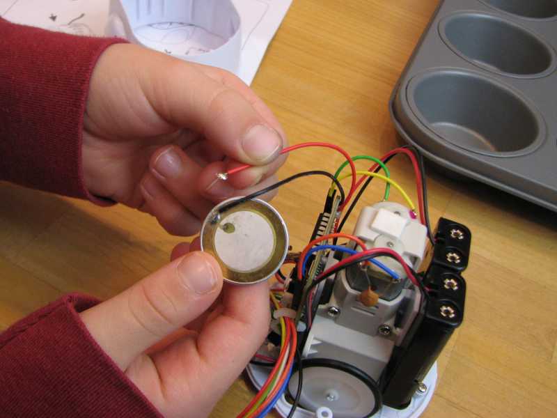
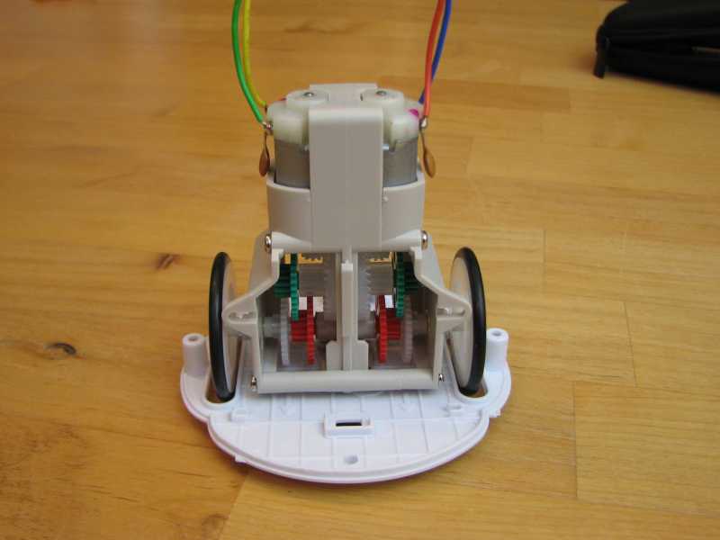 The robot is built around a drive train, the pieces for which are separately bagged. This suggests it’s common to other robot kits. Though the assembly instructions were clear, the gears were fiddly to assemble. At one point, we managed to undo almost all of our previous work when we tried to slip the last gear onto its shaft. No matter; we were able to put it back together. At this point in the assembly, with a drivetrain and a bottom plate, the possibilities of hacking this robot became clear.
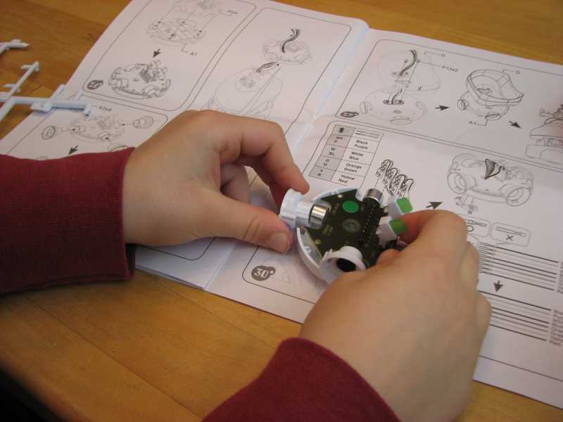
 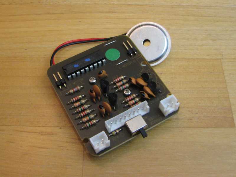 The controller for the robot comes preassembled. The IC on top of the board is a microcontroller. It is house-labelled for Elenco, but I suspect it’s a standard part with custom firmware. The manual has a schematic, so I compared the pinout to PICs and AVRs without finding a match. Maybe it’s a 68HC05 or another small micro. The assembly drawing pictured a socket under the microcontroller, but no such luck on this production unit. (By this time, I was started to get intrigued by the modification possibilities for this little robot.)