Building the AK5388 ADC breakout board

“Honey, the package you’ve been waiting for from Hong Kong is by your computer,” said my dear wife shortly after I got home from work on Friday. Even better, a few minutes later she suggested that I spend the evening in the basement, building up one of my new boards. I have a wonderful wife!

The AK5388 ADC breakout boards finally arrived!  I had a hard time waiting for them. First, Itead Studio didn’t ask me to correct the design until the day the finished boards were supposedly going to ship. (They did apologize for the delay — it sounded like there was a communications snafu between them and the fab.) Then I waited five more days for the board to be fabbed. Shipping from Hong Kong to Ohio took ten days. Looking around on the web, I’ve seen shipping times reported from seven to ten days, sometimes going up to as much as 20 days during the holiday season.

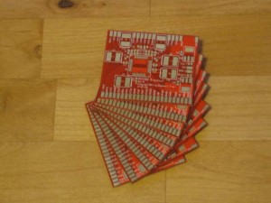
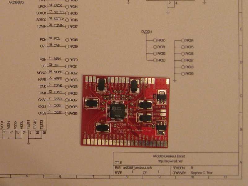
All eight boards look great. Other people who tried Itead reported some over-etching and silkscreen problems, but I don’t see any defects on mine. Since Itead now does 100% electrical testing, I have confidence that the boards will all work. I could spot the tiny dimple in each pad where the flying probes touched down, so it is clear that all eight boards were tested.

I went to the basement and heated up the soldering iron. The board went together easily. The 0.80 mm pitch of the AK5388 was downright easy to solder after the 0.50 mm  A3PN250 FPGA and other fine-pitch parts I’ve been using at work. Besides, I’ve learned some new soldering techniques lately that helped me solder the AK5388 quickly, but I’ll have to share those in another post. I did use a meter to check all of my AK5388 solder joints, though. There were a few bridges, but they cleaned up without a problem.

The pads for the big electrolytic capacitors are larger than necessary. I used PCB’s default EIA7343 footprint. The pads had plenty of room for the soldering iron, but they could have been smaller without sacrificing ease of assembly. (Did I use the wrong footprint once again? 0805 capacitors seem to be the only ones I get along with…)
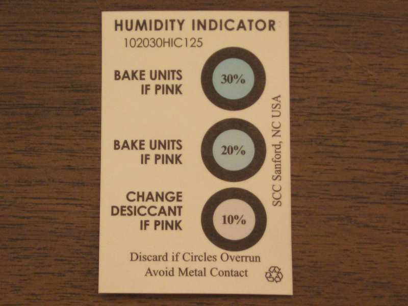
Lately Digi-Key has been taking much stronger steps to control moisture uptake by the semiconductors they sell. Instead of just shipping some cut tape in an anti-static baggie, they now seal the chips in an airtight bag with a packet of dessicant and a humidity indicator. I opened the bag this one was in about 4 weeks ago. Not bad so far, considering it was in my not-very-dry basement that whole time. Moisture uptake is important for reflow soldering techniques, but as far as I can tell, it is less significant for hand-soldering.
Now I’m left asking myself what comes next. In my original plan, the next step was to couple the ADC to the FPGA, put a USB core on the FPGA, and build a sound card. Once that works, adding a local oscillator and a quadrature mixer will make everything I need for a PC-based software-defined-radio (SDR) receiver, and this long trek will finally result in a radio.

However, I hear that the bands are great these days, and I’m not sure I want to take the time to homebrew an SDR rig just to get on the air. Maybe I should spend some time on a faster route to a radio, then come back to the SDR. I’ll probably have more on that idea next week.

Until then, keep on tinkering, and as always, your comments are welcome!
AK5388 ADC breakout board update

For the last month or two, a breakout board for the AKM Semiconductor AK5388 analog-to-digital converter has been my main project. Here’s an update on where it stands.

When I last posted about the board, I was waiting for parts to arrive so I could check their fit on a printout of the PCB. After the capacitor footprint error on the FPGA breakout board, I was feeling a bit cautious. The parts arrived and fit fine!  I checked out the ADC on its QFP footprint, and it was perfect. Then I tried the big capacitors on their EIA 3216 footprints, and those were fine, too.

Fixing the schematic

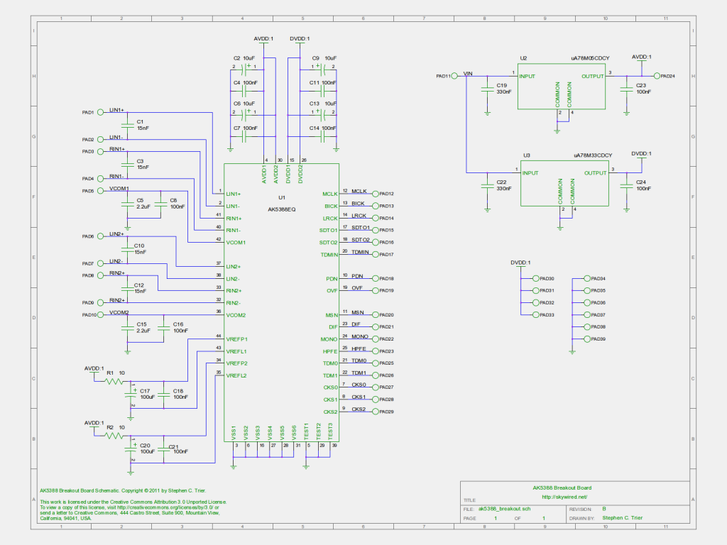
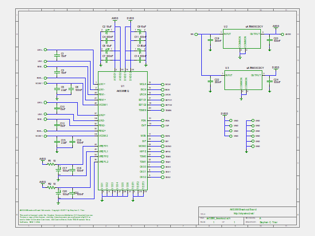
AK5388 breakout board schematic, revision B

I ran into some problems with the schematic when I did the PCB layout. One problem was that multiple pads named “GND” or “DVDD” were consolidated into one. A second problem was that the names I had assigned the pads were not visible in PCB, meaning I was in for a slow process of finding each one on the schematic in order to add the right label to the PCB’s silkscreen. I found a great solution, though.

The fix to both problems was to name the nets, not the pads. I restored all the pads to their boring PAD1, PAD2, … reference designators and named the schematic nets after the signals. Now, when I hovered the cursor over one of the pads in PCB, a little tooltip popped up and told me the net name connected to the pad, among other things. Labelling all of the pads took only a few minutes. I wish I had known about this trick when I did the A3PN250 FPGA board!

Secondly, using conventional reference designators to name the pads solved the problem with the DVDD and GND pads.

These changes resulted in the rev B schematic. A PNG version is above, and I’ll post the editable gschem version on the AK5388 breakout project page.

I have ordered the boards, and I will have more to say about that next week.

What do you think? Comments welcome!

PCB routing techniques for ADCs

PCB layout is fun, especially when you are trying to eke the best performance out of a component.  Last week, I finished the PCB layout for the AK5388 analog-to-digital converter (ADC) I chose for my digital ham radio transceiver project. Let’s take a closer look at some of the design details…

My top priority was to keep digital lines away from sensitive analog signals. The quickly-switching edges of digital signals carry lots of high-frequency components, which readily couple into any neighboring line. It’s best to keep this high-frequency crud away from quiet analog signals. It’s not great to let it couple instead into other digital lines, but digital inputs are pretty tolerant to it and rarely have problems.

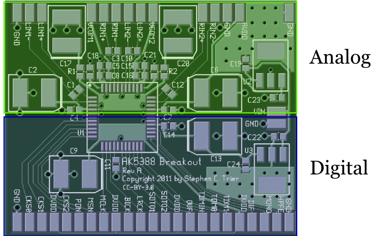
AK5388 board with an overlay showing how the analog and digital sections are separate.

The AK5388 pinout helps a lot with this separation requirement. As is done in many ADCs, all of the digital pins are on one side of the chip, and all of the analog pins on the other. When laying out a mixed-signal board (that is, one that has  both analog and digital elements), I like to draw a line across the board before I even start to place the parts, with all analog components going on one side and all digital on the other. As the placement and routing progress, that line will move and may even change into a zig-zag, but the idea remains: Keep the analog stuff on one side and the digital on the other.

On the AK5388 breakout board, the analog-digital border remains a straight line. Everything in the top half of the board is analog, and everything in the bottom half is digital.

Another reason to have a clean split is the return currents and their IR drop. Remember that current flows in a loop. When any of those digital lines changes state, it charges a small capacitance at the other end, and the current used to do that charging flows back through the ground plane. At high frequencies, that return current is largely confined beneath the digital line that caused it. On top of that, the return current causes a voltage gradient underneath it, thanks to Ohm’s law and the resistance of ground. (V = IR)  This voltage gradient can act as an additive noise source on analog signals that are routed near it. The careful split in this board’s design will help keep the digital return currents from affecting the analog signals.

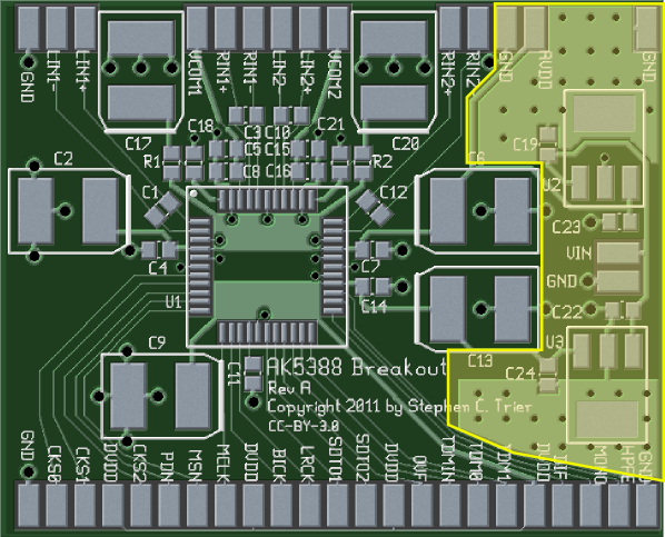
Another feature of the board is that it has local analog and digital power supplies for the ADC. The power supplies are located in their own area, again to try to limit noise caused by the return currents. In the picture below, the power supplies are highlighted in yellow.

The AK5388 breakout board with the power supply location highlighted.

The voltage regulators used here (uA78M33CDCY and uA78M05CDCY) are in SOT-233 packages, which have a large lead on one side to help with heatsinking.  The board is laid out with some extra copper area to act as a heat spreader for each SOT-223, along with a bunch of vias tying the top-side copper to the ground plane. These vias have a thermal role, not primarily an electrical one, as they help transfer heat from the top-side heat spreader down to the ground plane to further spread it out.

Although there are ways to estimate the thermal performance of a heat-spreader design like this, I didn’t do them. Frankly, I don’t have any idea whether this board’s thermal provisions are adequate. Even at the bargain price of $5/square inch to have this PCB fabbed, adding copper just for thermal management gets expensive. If the heat-spreading area turns out to be insufficient, I’ll find a way to attach a heatsink to the top side of the regulators, solder a piece of brass to their large lead, or something along those lines to remove the heat more efficiently.

Finally, take a look at the decoupling capacitors. C4, C7, C11, and C14 are 100 nF capacitors, each on one power-supply input to the ADC. They are positioned as close to the ADC as I could manage. One could argue that their positioning is not quite perfect because there is a relatively long path from their grounded side to the closest ADC ground pin. It goes through two vias and the ground plane. I have never looked into whether this makes a significant difference. If you know, leave a note in the comments and tell me!

In any case, the 100 nF capacitors are multi-layer ceramic capacitors (MLCC), which have a low equivalent series resistance (ESR) and inductance (ESL). Those characteristics make them ideal for decoupling high-frequency noise on the power supply lines.

Next, C2, C9, C22, and C23 are big 10 μF decoupling capacitors. These are positioned a little farther away. They are aluminum electrolytic capacitors, which have a higher ESR and ESL than ceramic caps. (10 μF ceramic capacitors are expensive!) These capacitors are better for removing low frequencies, including the audio range, from the power supplies. For that reason, I did not see much harm in putting them a little farther from the ADC, with the extra inductance and resistance that implies. Besides, these things are BIG! If they were any closer to the ADC, routing the signal lines in and out would get pretty challenging.

One trick for getting the decoupling capacitors closer is to put them on the back side of the board. The distance through a via would be much shorter than the distance needed here. I wanted a single-sided design here, so that wasn’t an option, but it’s something to keep in mind.

I won’t claim that I know everything about designing for a high-performance ADC. In fact, it’s possible that someone more experienced is planting their face in their palm right now, saying, “I can’t believe he did that!”  (If that’s you, by the way, drop me a note to let me know what the problem is, would you?)  That said, what I did here is based on app notes and other materials from a number of semiconductor companies, including Analog Devices and National Semiconductor, and I think it’s pretty sound.

I ordered the parts for this board today. It doesn’t take long for UPS to get things to Ohio from Digi-Key’s home in northernmost Minnesota, but it’s always a long wait when I’m itching to try something out.

I’ll catch you next week with more on electronics, DSP, and ham radio.

PCB layout for the AK5388 ADC breakout board

I had some time to myself this weekend and was able to get the AK5388 breakout board routed. The board carries an AKM AK5388 audio DAC, which has 24-bit output and up to a 123 dB signal-to-noise ratio. My plan is to build up this board, evaluate it to verify that it works as I expect, then use it as the ADC stage in a DSP-based ham radio receiver.

Moving the schematic from gschem to PCB was really easy. This was my first time using PCB’s “Import schematics” command. It was a breeze, especially compared to the old way of doing it, the gsch2pcb command. That command worked well enough, but I could never get it done without checking the documentation or a howto online. “Import Schematics” required no such thing. Bravo to the PCB developers!

As with the FPGA board, I laid out the board with a solid groundplane on the back and all components and traces on the front. That way, it can be placed on a piece of copperclad board, for skywired construction, without risk of shorts to ground. It’s also good for noise performance.

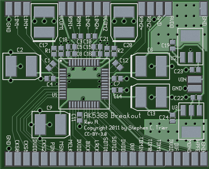
Photorealistic view of AK5388 breakout board, top side

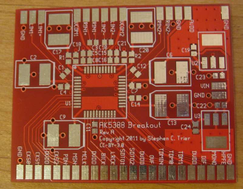
The square chip in the middle (QFP, U1) is the AK5388. On the right edge are a 7833 and a 7805 voltage regulator, for the digital and analog power supplies, respectively. The board includes some heatsink area around the regulators (U2 and U3), with thermal vias to stitch the heatsink to the groundplane on the back. The rest of the components are decoupling capacitors, lots of decoupling capacitors, plus two resistors that also help control noise. A 24-bit ADC needs quiet power supplies!

As you might expect, the bottom side is kind of boring:

Photorealistic image of the bottom side of the AK5388 breakout board

That’s the ADC board so far. Although I have Gerber files now and could go order the boards, I’m going to order the parts first this time and test-fit them on a printout of the layout.

AK5388 audio ADC breakout board design

A few weeks ago, I picked the AKM Semiconductor AK5388 as the analog-to-digital converter for my receiver design. This high-performance audio DAC has a 24-bit output with up to 123 dB signal-to-noise ratio (A-weighted).  I hope that the narrower bandwidths of a communications receiver will beat that. The idea is to do the automatic gain control (AGC) in digital, so that the receiver will not need an analog AGC loop. I hope that a preamp or attenuator at the front end will be enough to make up for the limited dynamic range of the AGC.

Now, I am aware that getting performance like that requires great care in the details of the design and layout, but if this wasn’t a challenge, it wouldn’t be nearly as much fun!  The AK5388 datasheet does give me some concern, because it does not make much mention of the techniques needed for a high-performance DAC. Admittedly, datasheets from Japanese manufacturers are often thinner on details than those from the leading US suppliers, and this one is much more complete than some. On the other hand, it may be that the datasheet is glossing over any coddling this chip will need.

There is one way to find out, and that is to start breadboarding. This is a surface-mount part, so I have designed a breakout board very much like the board I built for the Actel Microsemi A3PN250 FPGA. The schematic is below.

AK5388 ADC Breakout Board schematic

The schematic largely follows the “System Design” section of the datasheet and the example of the AKD5388-A evaluation kit (PDF). It’s not strictly a breakout because I included on-board analog and digital power supplies. An ADC like this needs quiet, local power, so I picked some reasonably quiet supplies and put them on-board. I chose 7800-family regulators from TI because they have reasonable noise specifications. I almost went with other choices that were explicitly designed for low noise, but they were quite a bit more expensive for not much less noise. The AKD5388-A kit uses an uA78M05 and claims to be able to obtain the full dynamic range of this ADC, so there is little reason to spend more at this point.

I’m using the analog power supply as the voltage reference. I considered a dedicated reference, which would be more expensive but perhaps lower noise. Here, too, I followed the lead of the evaluation kit.

The PCB layout should be straightforward. I like to build by skywiring components over a groundplane, so this breakout board will be designed to sit directly on a groundplane, with all components and connections on the top side. All external wiring points will be pads on the PCB, ready for soldering, just as with the A3PN250 FPGA board.

I’m excited about trying out this part. What do you think? Comments welcome!

Papilio One Xilinx FPGA breakout board

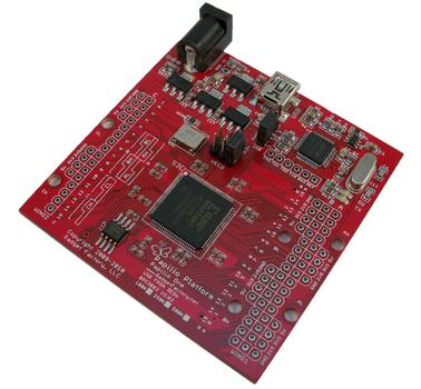
This week, I came across the Papilio One FPGA board. This intriguing board mounts a Xilinx Spartan 3E, in either the 250K or 500K gate flavor, along with power supplies and an on-board USB programmer.  It’s inexpensive, at $50 for the 250K version and $70 for the 500K version. This would make a good pre-assembled alternative to the Microsemi SOC (née Actel) A3PN250 breakout board I am using.

One really neat feature of the Papilio is that it is designed to be Arduino-compatible! By loading an AVR8 soft core onto the FPGA, Arduino-compatible sketches can run on the board. The board supports a set of connectors to which up to 6 expansion boards (“wings”) can be attached, similar to shields. Its inclusion of a programmer and power supply also imitate the Arduino model.  As well as Arduino programs, the board is also programmable in Verilog and VHDL.

Unlike my board, its off-board connections are through-hole, and it can’t be mounted directly on a ground plane without extra insulation.  I like the philosophy of bringing out a full 48 uncommitted pins to the off-board connectors instead of loading up the board with extras.  Boards with RAMs, flash, and displays are easy to get started with, but end up being confining, making it harder to add external circuitry when the on-board stuff is not enough.

The Papilio is a close relative of the Open Bench Logic Sniffer, designed by Ian Lesnet and Jack Gassett. The Papilio heritage shows in the Logic Sniffer’s two “wing” expansion connectors.

If your FPGA preference is Xilinx or if you want a flexible, basic breakout board with an on-board programmer and power supply, the Papilio is well worth a look.

The iambic keyer core is alive

With just a few tweaks, I brought up the “IambicV” iambic keyer core on one of my A3PN250 breakout boards. I was stunned when it made dits, dahs, and iambic dah-dits perfectly the first time out. Yes, I know that’s what a testbench is supposed to make possible, and yes, I’ve had it happen before, but I still always expect smoke the first time I turn something on.

I made a few changes from last week’s version.

With just a few tweaks, I brought up the “IambicV” iambic keyer core on one of my A3PN250 breakout boards. I was stunned when it made dits, dahs, and iambic dah-dits perfectly the first time out. Yes, I know that’s what a testbench is supposed to make possible, and yes, I’ve had it happen before, but I still always expect smoke the first time I turn something on.

I made a few changes from last week’s version. One change was to invert the dit and dah pins. Although high-true logic is convenient within the keyer module, it seems like a good idea to have the actual paddles grounded, so the inputs had to be low-true. The physical constraints file enables the built-in pull-up resistors on the dit and dah pins.

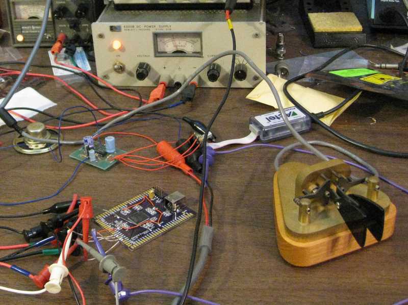
For an audio amplifier, I used an old Saint Louis QRP Society LM380 board.

It’s all lashed together on my bench, but it works.

To download the core, see the iambic keyer project page.