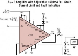
 This week I want to share a new favorite chip of mine, the LT1970 power op amp from Linear Technology. This nifty device runs from a 36 V supply and can source or sink 500 mA. That’s not too unusual, but how about programmable current limiting, outputs to indicate over-temperature and over-current, and more? Think of it as a four-quadrant power supply on a chip, or as the source part of a source measurement unit.
The first nice feature of the chip is the programmable current limit. The chip has two inputs, one for sourced current and one for sunk current, that accept a voltage from 0 V to 5 V. It compares these voltages against the current measured across an external sense resistor and limits its output when the measured current exceeds 1/10 the voltage on the relevant control pin. Differential input pins, independent of the output pin, are provided for the sense resistor.
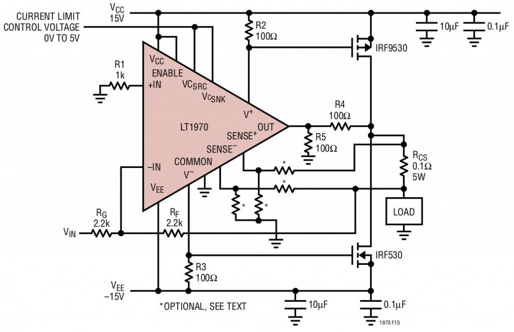
Another great feature is that the output stage has its own power pins. One of the neater “trick” circuits out there is to boost the current capability of an op amp by using the power supply pins to drive external transistors. An ordinary op amp without separate power pins can also be used this way, but the bias current of the external transistors will be proportional to the op amp’s quiescent current, which means one will probably need a low quiescent current model. By pinning out the output stage’s power pins, the LT1970 makes it easier.

This circuit ends up running the output transistors in class AB. The bias current in the transistors is controlled, in part, by the quiescent current of the op amp. When the op amp tries to increase the voltage of its output, it will deliver more current to the output, pulling that current from its power supply. That, in turn, changes the voltage on the base of the upper external MOSFET, causing it to source more current as well. The equivalent happens when the op amp needs to sink current.
Another advantage of choosing the LT1970 for this configuration, instead of an ordinary op amp, is that all stages except the output stage will see a stable power supply, keeping the PSRR up where it belongs. As for the last stage, when combined with the external transistors, it resembles two Sziklai pairs (also called “complementary Darlingtons”) biased into class AB.
The separate power pins also make it easy to use a lower-noise supply for the input stages and a high-current supply for the output. I used them for another purpose: My application needed a wide input range but drove an input sensitive to overvoltage. Running the input stages off of 24V and the output stage from a lower voltage ensures the output will not hit an unsafe value. Watch out, though, because V+ and V- must be within the VCC and VEE supplies to the op amp’s input stages.
Another neat feature is three open-collector outputs that indicate that the op amp has gone into thermal limiting, into current source limiting, or into current sink limiting. These pins can drive LEDs for an easy status display.
The biggest drawback of the LT1970 is its package, a 20-pin TSSOP with a thermal pad on the bottom. That thermal pad means you pretty much have to have either a hot air or reflow setup to solder it.
As you might expect for a part like this, there are ways to use it beyond the obvious. The current-limiting flag outputs can be used for snap-back current limiting, where the output current is sharply reduced after it enters limiting. The current sense pins can be used as voltage-limit inputs, enabling circuits like a symmetric, voltage-controlled limiter. These ideas are from the data sheet; I haven’t tried my creativity at coming up with other ways to (ab)use the chip.
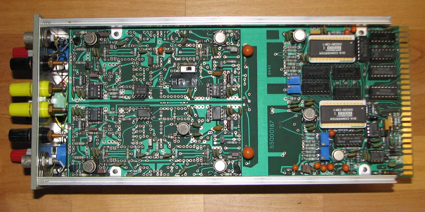
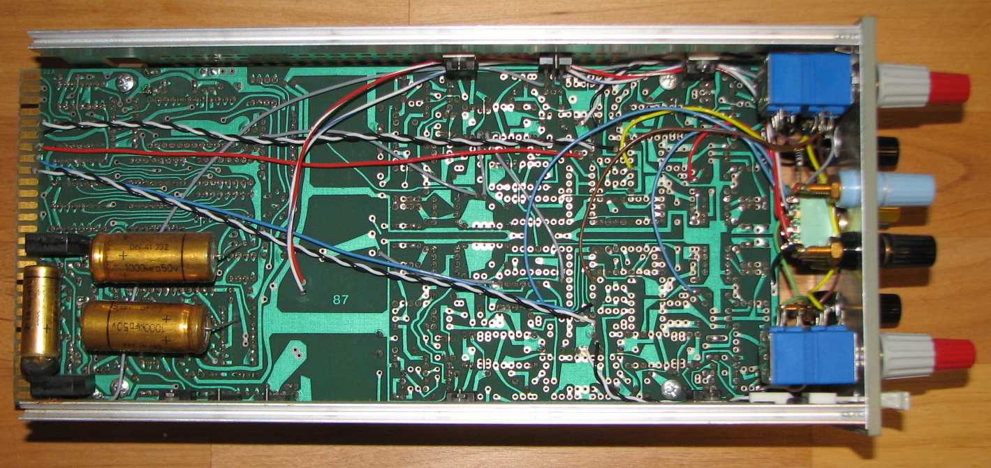
No, I used the chip for a boring old power supply. It was a two-quadrant supply, though, meaning (in this case) that I needed a positive-output power supply that would either source or sink current to maintain its output voltage. The voltage was controlled by an analog input. What I needed was basically just an op amp with current limits and a few hundred milliamps output. The LT1970 was perfect. I fitted it with potentiometers to adjust the current limits, a set of LEDs for the status outputs, and as much PCB copper as I could manage for a heat spreader. I also included some compensation for capacitive loads. It worked great. I haven’t had any issues with oscillation, the LEDs have been handy to tell me when I mess up, and the current limit has saved my bacon at least once. Sure, I could have built the same supply from separate parts for a lower cost, but it would not have been nearly as easy or as quick. This is another case where it was worth spending a little money on a chip in exchange for saving a little engineering time.
The feature I miss most from the LT1970 is a current amplifier output. It does current measurement internally, for the current limit feature, but a voltage proportional to current is not brought out. For my power supply, I had to add an external difference amplifier to measure the output current. The difference amp used the same current sense resistor as the LT1970, but it would have been nice to have that function built in.
The quantity 1 price for the LT1970 is $9.88 from Digi-Key or $6.05 directly from Linear Technology.
Figures: Copyright 2002 Linear Technology Corporation. Used by permission.
