Making progress on the A3PN250 FPGA breakout…

I’ve made lots of small steps on the A3PN250 FPGA breakout board the last two weeks.

Firstly, I built an JTAG adapter cable to work around a wiring error on the PCB. When I laid out the board, I accidentally numbered the pins on the JTAG connector DIP-style instead of ribbon cable style.  That meant that all the pins except for pin 1 were wired wrong. After thinking a bit about the options, which included scrapping the board and starting over, or skywiring in corrected wiring for the connector, I decided the cleanest solution was to make a custom JTAG cable that moved the pins around where they belong. I’d seen other cables built this way. I asked myself, “How hard could it be?” Continue reading “Making progress on the A3PN250 FPGA breakout…”
Building the ProASIC 3 nano FPGA board

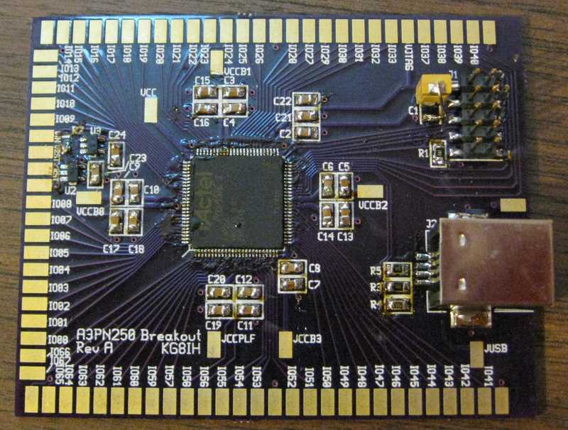
After a busy week spent traveling for work and a morning digging out from a surprise snowstorm, I had a great weekend with my family. It was Sunday night before I heated up the soldering iron and got down to business building the ProASIC 3 nano FPGA board.

I started with the toughest component, the FPGA. Its central location and low height means ….

After a busy week spent traveling for work and a morning digging out from a surprise snowstorm, I had a great weekend with my family.  It was Sunday night before I heated up the soldering iron and got down to business building the ProASIC 3 nano FPGA board.

I started with the toughest component, the FPGA.  Its central location and low height means that I will have an easier time accessing it before other components are mounted.  That is not likely to be a big problem for this board, with plenty of space around the chip, but I would still prefer not to have to work around the filter capacitors if I can avoid it.  On the other hand, its 100 pins and 0.5 mm pin pitch makes it far and away the most difficult soldering job on the PCB.

Continue reading “Building the ProASIC 3 nano FPGA board”

FPGA Breakout Board Layout

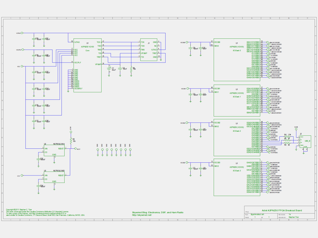
Here at last is the printed circuit board layout for the FPGA breakout board. I’m planning a series of projects involving FPGA-based DSP for ham radio, and in order to build them, I need an FPGA and a PCB on which to mount it….

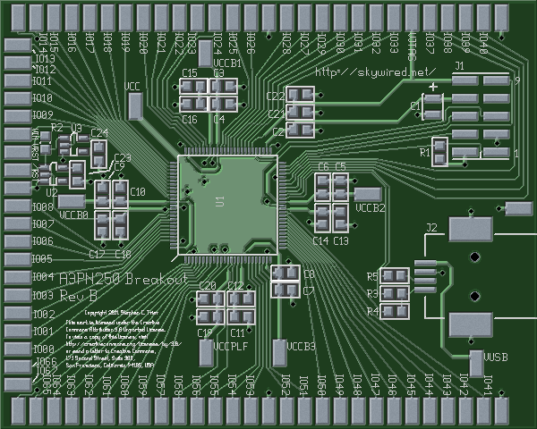
The goals for this layout constrained it to be a nearly single-sided layout, …

Here at last is the printed circuit board layout for the FPGA breakout board. I’m planning a series of projects involving FPGA-based DSP for ham radio, and in order to build them, I need an FPGA and a PCB on which to mount it. In the last installment of the project, I presented the schematic for the breakout board.

The goals for this layout constrained it to be a nearly single-sided layout, with a ground plane on the back. That way, the board could be mounted directly on a piece of copperclad with no short circuits to ground. My budget limited me to a double-sided board, so all signal and power traces had to go on the top side.

That said, here is the layout, top and bottom.

FPGA breakout PCB, top side

Continue reading “FPGA Breakout Board Layout”