BITX 40!

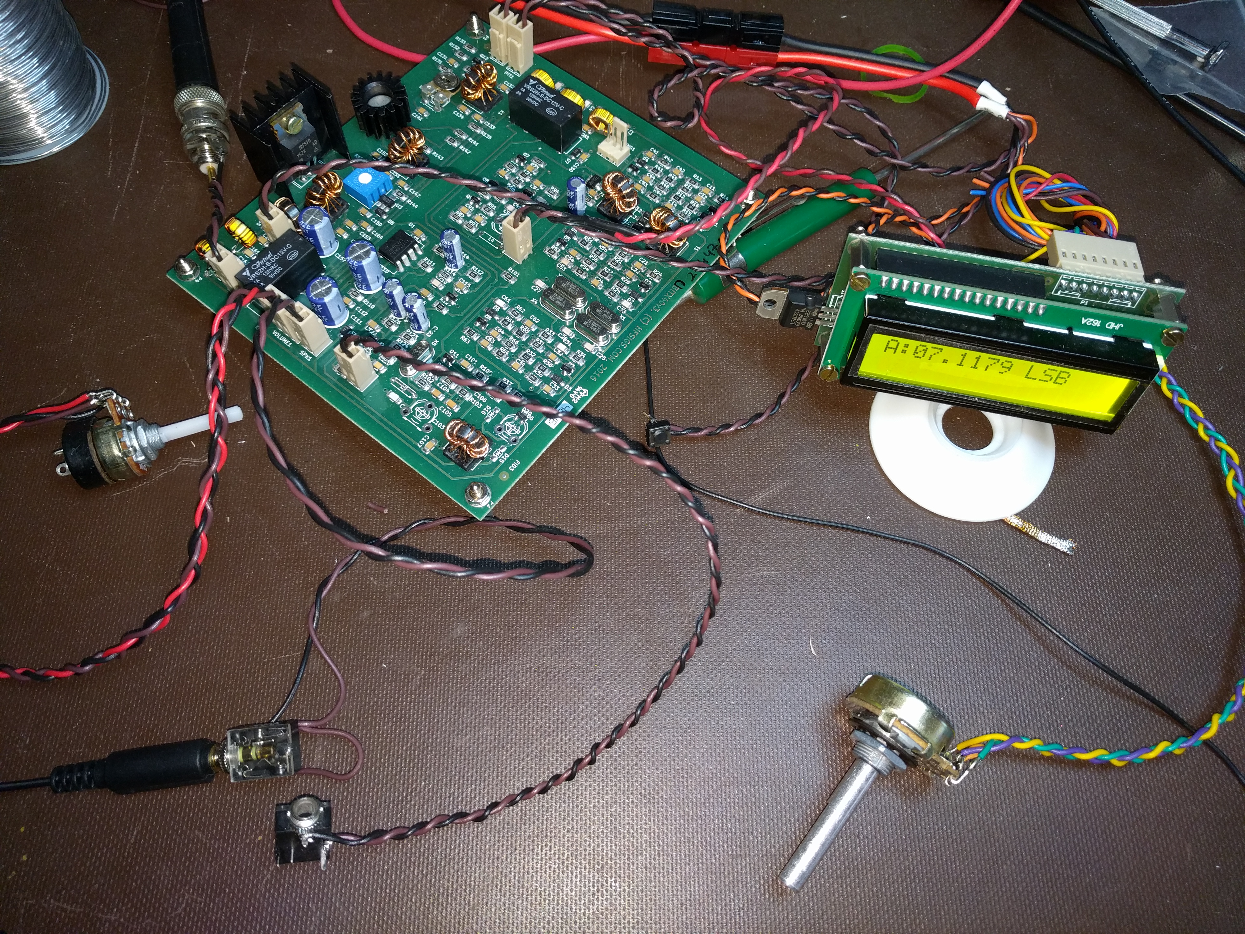
I’ve decided to build a BITX 40. This petite SSB transceiver sells for a mere $59, some assembly required. As it comes, it puts out approx. 7W, and with some straightforward upgrades it can produce 25W. It comes as a fully-assembled PCB plus most of the parts needed to hook it up. A case, speaker, and a few other incidentals are not included. The board and radio are designed to invite hacking and customization. It is also designed to serve as an introduction to homebrewing for hams who may not be ready to build a radio from scratch. For more information on the BITX-40, see its supplier http://www.hfsigs.com/ and the active and helpful support community at groups.io.

My BITX 40 is operable “al fresco” on my workbench. The included Arduino/Si5351 VFO works fine and tunes the full 40m band. It needs a little bit of work before I can transmit with it. It’s important to understand that the BITX 40 is not a turnkey rig. Many of them ship with small flaws, and figuring out and fixing the flaws is part of the fun. (This is why that helpful community at groups.io is so important.) Mine shares a flaw with Wayne, N6BM’s BITX 40 — the BFO frequency is inside the IF passband, instead of about 300 Hz below the passband like it should. This means that stations I tune sound bassy, I can hear part of the opposite sideband, and when I transmit, the carrier is not suppressed.

(I suppose I could call it “vestigial sideband”, like what NTSC TV uses, but it’s supposed to be SSB…)

Wayne fixed the problem by changing a capacitor in the BFO circuit to pull the frequency where it needed to be. I plan to fix it by disabling the analog BFO and instead use a spare Si5351 output. Having a tunable VFO will let me put the passband exactly where I want. With a little more code, it will also give me passband tuning.

I think I found a bug in the microphone amp that I’m going to take a closer look at, and I found a perfect case at the Mike and Key hamfest in Puyallup last month. I didn’t even try to negotiate the price. It was free!

I’ll have more on my BITX 40 project in upcoming posts.

Some thoughts on the K5BCQ Si570 signal source

For the last few months, I’ve been working on building a radio from a pair of kits old enough to vote: KK7B’s R2 receiver and T2 transmitter. A complete transceiver built from these kits needs some other pieces, including a VFO (variable frequency oscillator). After looking around a bit, I picked an Si570 signal source kit from Kees Talen K5BCQ and John Fisher K5JHF.

Si570 signal source and frequency counter, showing 17 Hz difference at 10 MHz

I’m not going to try to review the kit, because Jack Smith wrote the canonical review of it already. Instead, I will share some impressions of the kit.

First off, the PCB layout has not gotten better. There are some crazy things about it, including through-hole parts mounted on opposite sides of the board, such that one component prevents access to the terminals for another. The layout of the output circuit is also odd. In an effort to provide for many different output options, apparently while keeping trace lengths to a minimum, the output section is crowded and hard to navigate.

I had to do only a little debugging after assembly. The first problem was that the two pads at the ends of the Si570 were not well-soldered. Jack Smith ran into the same problem. My second problem was a little more subtle. I fired up the circuit and saw output at the right frequency, but 0.5 V in amplitude. I purchased the CMOS output option, so it should have been a 3.3 V square wave. Tracing out the circuit, I found that the signal was getting knocked down when it passed through a DC blocking capacitor. Oddly enough, I noticed that when my ‘scope probe pushed down on the right spot on the capacitor, the output jumped up to 3.3 V. I probably fractured the cap with the heat of soldering. I had changed my mind about capacitive coupling anyway, so I replaced the cap with a 0 ohm resistor and now I get the output I expect.

Waveform from the Si570 VFO

The ‘scope shot shows the output, which is a reasonably clean 3.3 V CMOS signal. There is almost a volt of overshoot on the transitions, which is a little concerning, but I am not too worried about it at this point. The CMOS edges are fast, making overshoot understandable, and the size of the overshoot is likely to change as the VFO is integrated into the radio. I will worry about it later.

All in all, I have to say that the board works a treat. It is awesome to see 1 Hz tuning resolution and crystal oscillator stability coming out of a tiny 8-pin surface-mount part. I measured the frequency as being off by about 14 to 17 Hz at 10 MHz, which works out to about 1.7 ppm. Drift is confined to that 3 Hz range, at least when sitting on my basement workbench. The board does have a provision to calibrate out the frequency error, which I have not used yet. This much error really doesn’t matter.

The microcontroller firmware with the kit works well. The user interface is slightly unusual, with a decimal point used as an input cursor, but it works fine in practice. I do wish there was a way to configure band limits. The board has provisions for band selection, with up to eight bands possible. However, regardless of the band selection, the device will tune over its entire range. In a multi-band radio that is a poor idea, because it would be too easy to transmit at the wrong frequency and damage the final amplifier. With hundreds of on-board memories (100 per band, minus 20 reserved for setup), it would be nice if a few configuration memories were used to choose tuning limits for each band.

Over all I am happy with the board. It will serve just fine as my VFO.

Working slowly on the R2/T2 radio

I was at my workbench when my son came downstairs to talk and hang out. A budding reader, he soon started singing the A-B-C song with the letters mixed up. It crossed my mind that this was odd, but I didn’t think much about it until I heard

That rang a bell, and suddenly I realized he was singing my oscilloscope’s front panel. Music by Mother Goose, lyrics by Tektronix.

When he came downstairs, I was working on assembling the K5JHF/K5BCQ Si570 synthesizer kit. It turned out to be a bit fiddly, but it is a decent kit. That said, I would not lay out a PCB like this one. It has a number of vias in the middle of pads, and while that’s not a big problem for hand-soldering, I would avoid it in a PCB as a matter of good practice. You never know who might decide to use solder paste and reflow to assemble the board, and then those vias will be trouble.

Worse, though, is the positioning of the connector for the LCD. It is laid out smack in the middle of the footprint for the microcontroller, but on the opposite side of the board. If you look at the big black socket in the picture above, you will see the back side of the microcontroller’s pins poking through the board on either side of it. This positioning means one has to solder the header on one side of the board, then insert the micro on top of the pins one just soldered, flip over the board and solder the micro’s pins next to the header. The header pins are non-serviceable once the microcontroller is installed, and the microcontroller won’t be easy to get out, either. DIP desoldering tools won’t fit with the header in the way. I’m not sure why the board is laid out this way, except that it makes the board a little smaller. Maybe that was the only concern.

At this point, it’s fully assembled except for the encoder/switch, which is about half wired. What am I doing blogging? I could be soldering!

An Si570 VFO for the R2/T2 transceiver project

I’m continuing to work on my R2/T2 transceiver project as time allows. My goal is to get on the air before the sunspot cycle peak passes. That gives me a little time yet, but at the rate I get things built around here, it’s going to be a close race.

Even when building a radio from kits, as I am here, there are many decisions to be made. When I bought the KK7B R2 and T2 kits, I had no thoughts about what to use for a local oscillator. Technology has advanced mightily since then, and now I have the option of an Si570 frequency synthesizer. This little chip provides a precise, low-noise  digital clock at programmable frequencies between 3.5 MHz and 1.4 GHz, depending on the variant one buys.

After looking around a bit, I picked John Fisher K5JHF and Kees Talen K5BCQ’s SI570 controller/frequency generator kit. Once it arrived, I had trouble figuring out how to fit it into my case. This case has a 0.125″ thick aluminum front panel. The threaded bushing on the kit’s encoder/switch was not long enough for this thick panel and a mounting nut, let alone a washer. There were also some mechanical things I didn’t like about the circuit board. I thought a bit about designing a new board for the parts from the kit, but I decided I could fix the worst of the problems with a new encoder. A little browsing at Mouser turned up an extremely similar model that had the longer bushing I needed. It even has the same footprint.

I’m a little stumped by how similar they are. The Mouser one (on the right) is from Bourns, but looking over the data sheet, I couldn’t find a model with a bushing and shaft length matching the one from the kit. The body of both units is essentially identical. Hopefully they are electrically close enough, too. I had to guess at how many pulses per rotation it should have.

I’m still chewing on another mechanical question. The kit is designed to have the PCB soldered to one end of the LCD, with the encoder mounted off the PCB, on the right of the LCD. I want to have the tuning knob centered below the LCD, so the PCB is going to have to stay with either the LCB or the encoder, and the other will have to be connected with wires. My initial thought was to mount the encoder on the PCB and wire the LCD remotely, but I’m beginning to favor mounting the PCB on the LCD and running wires to the encoder. The connection between the PCB and LCD will involve high-frequency digital signals, while the connection to the encoder is analog switch closures that have less potential for RF interference. It would be better to have the LCD signals cover a shorter distance so they radiate less.

On top of that, putting the PCB and the LCD together will make it easier to surround them with a shield.

All this rambling aside, yes, I’m making slow progress on the R2/T2 rig. When I’m working on a project, sometimes I spend a lot of time doing and other times I spend my time thinking. I’m a little out of my element with the mechanical design of the radio, so lately I’ve been planning the design carefully.

An enclosure for the R2/T2 transceiver

After months of organizing parts, I have finally gotten back to the R2/T2 transceiver project. Don’t get me wrong, the cleaning and sorting is not done, but I felt the urge to do something a bit more… constructive.

While cleaning, I found a box of old electronics junk that had promising cases. Electronics enclosures are expensive. Salvage can be a good way to keep the cost down. I don’t know what this thing once was, but there are military-style circular connectors on the front and back, two fuse holders, a power inlet, and no visible controls.


Opening it up, I found this:

There’s a lot of empty space in there! It looks like it was some kind of power supply. Next to the weighty transformer and big blue filter cap, a circuit board carried 7805 and 7806 regulators, several current-sense resistors and an LM324 quad op amp. It also had a power transistor on board and connected to the big TO-3 transistor on the heat sink in the back.

The board on the other side had a couple of high-voltage film capacitors, some ten-turn pots with their positions set with nail polish, two LM324’s and one RCA 4151 voltage-to-frequency/frequency-to-voltage converter. Down in the lower-right corner, it also held a solid-state relay. I’m a little more stumped about what this board was for. Maybe it was more power-supply logic, or maybe some kind of controller.

Tracing out the wiring harness revealed that 120VAC is run to the front connector, with only a fuse between the connector and the power cord. That could get exciting quickly to anyone not expecting it.

I pulled apart the whole thing, salvaging only the transformer, two ICs, and some fasteners. I tried to salvage all the ICs, but some were corroded into their sockets and could not be extracted without breaking pins. I have not had that happen before.

That’s the final product. I left the fuse holders, the heat sink, and a common ground point in place. They might be useful when this box becomes a transceiver. The front and back panel are 0.125″ aluminum and slide out after a few screws are removed. It will be easy to replace them with new panels for the radio.

The only fixed surfaces in this box on which to mount things are a pair of narrow rails on each of the side extrusions. The bottom is removeable and isn’t set up well to hold circuit boards. I will have to either add a false bottom or come up with a way to mounting the boards at right angles from the sides. Putting the boards flat on the sides, like the original residents of this box, won’t give me enough room, and because the boards are not sized to fit the walls, I would have to improvise some kind of mounting panel or angled standoffs to hold them anyway.

In any event, that problem is solvable. It’s a nice case for what I hope will be a nice radio.

FDIM 2012: The YADI micropower digital interface

Next in our tour of projects from the Four Days In May event at the Dayton Hamvention is an innovative radio-to-computer interface.

The YADI rig-to-computer interface prototype

The unique feature of YADI, Yet Another Digital Interface, is a micropower VOX circuit. This lets it sip power while waiting for a signal, where other interfaces are less battery-friendly. The secret is that the VOX amplifier is biased in “class E”, according to its designer, Dana Browne AD5VC. (It is possible he meant class C, since class E amplifiers are tuned and a VOX amp is broadband.)  That means that the amp uses no bias current when there is no signal. Its biasing also causes it to rectify the input, eliminating the need for an additional rectifier. The quiescent current is less than the self-discharge current of a 9V battery. In other words, the battery loses more energy sitting on a shelf than this interface needs to keep idle.

Dana, with Jim Giammanco N5IB, designed it with an eye towards emergency communications, particularly after hurricanes in their home state of Louisiana. It is designed to interface any radio and to any computer sound card, to support the many digital modes available today.

A kit version of the interface is being produced by the Baton Rouge Amateur Radio Club. The kit version was also on display at FDIM, but unfortunately, my photos of it did not come out. Suffice it to say that the kit includes a good-looking PCB, features easy through-hole assembly, and fits in a mint tin. The price is $35.

Unfortunately, I can’t find a link for the kit, other than some copies of the manual on a file sharing site. The BRARC web site is a vacant placeholder, and Google turns up no other leads. I hope this worthy kit becomes available soon and gets the publicity it deserves.

KK7B R2 receiver: lifted pads, a scorched board, and it works anyway

I’m slowly making progress on my KK7B R2/T2 transceiver project. At my last report, I was waiting for replacement capacitors to arrive. They did, and I pulled out my ancient solder-removal iron, a Radio Shack unit from who knows how long ago.

Either my unsoldering skills are rusty or I was too impatient, or both. I managed to lift four pads, completely demolishing one. The other three were salvageable. I’d like the board to be perfect, but having it work is an acceptable substitute.

The new caps went in easily, with only a little fiddling to wire around the ruined pad. Better yet, the excessive bias current I saw before the replacement is gone! The board is supposed to be adjusted to 100 mA current. It used to start at 120 mA, with the bias adjustment set to its minimum, and drift its way up to more and more current from there (going as high as 200 mA before I’ve lost my nerve and switched it off). Now it starts at 84 mA and… drifts its way up from there to 130 mA and more.

OK, so one problem was solved. I can always increase current with the bias adjustment potentiometer.

After scratching my head a bit, I finally noticed one small sentence in KK7B’s articles on the R1 and R2. The audio output transistors need a heat sink, do they? Oops! I dug around a bit in my junk box but couldn’t find anything that would fit. The articles say the audio amp will drive a pair of headphones fine without the output transistors, so I decided to take them out.

I recently got a Sparkfun hot-air soldering station (a Sparkfun Free Day prize!) and thought I’d give it a shot. Sure, hot air is usually for surface-mount parts, but solder is solder, right?  Not being sure how to set the airflow and temperature settings, I set both on the high side, put some flux on the output transistors’ pads, and went for it. The result wasn’t pretty:

Oops... A scorched R2 PCB

Yes, I scorched the board. Oops. Between this and the lifted pads, I think I need to work on my unsoldering skills.

Since the transistors are 50 cent parts (TIP29/TIP30), I unsoldered them the easy way: I cut the leads, removed the leads from the board with my conventional iron, then cleaned out the holes with my solder sucker. I didn’t damage any pads this time!  (The picture above was taken after all of these steps.)

A little more soldering to hook up a BNC and some other goodies, and the board was alive!

R2 on the bench, surrounded by test equipment

That’s a Tek 191 signal generator as the VFO (variable frequency oscillator), with a frequency counter as the readout. That’s an MFJ QRP antenna tuner in the foreground.

I didn’t build a phasing network yet, so I drove only one VFO input. That causes the R2 to function like a conventional direct-conversion receiver,receiving both sidebands simultaneously. That said, it works. I was able to hear signals, though frankly many were quite hard to copy. I’m not sure what else might be wrong.

The frequency counter spits out a lot of digital noise. I learned to flip it on only to spot-check my frequency. It’s a lot quieter in standby mode.

Did I mention that IT WORKS?

Despite the success, I’ve been struck by a bit of paralysis in moving forward. There are so many choices to make for integrating the radio.

  • What kind of VFO should I use? Should I design my own or buy a kit?
  • Which modes should I include?
  • How much power output do I want?
  • What power amp should I use? Should I design my own or buy a kit?
  • Which case should all of this go in?
  • What microphone, and microphone connector, should I plan for?

Keep in mind that this is supposed to me my fast route to getting on the air, so I’m thinking kits for both the VFO and amp. Besides, with as busy as it has been at work lately, it is nice to sit back and just build something.

It’s not a pretty project any more, but it works! Hooray!