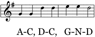
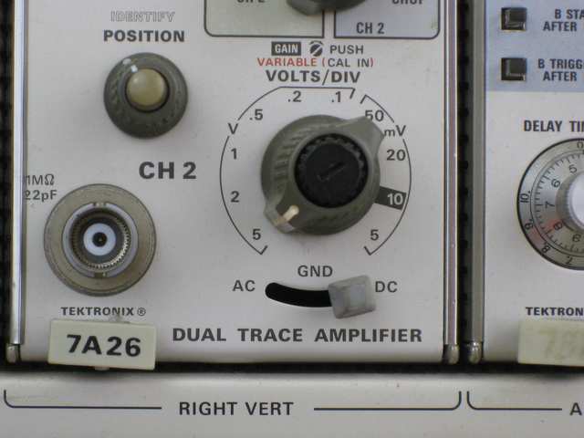
I was at my workbench when my son came downstairs to talk and hang out. A budding reader, he soon started singing the A-B-C song with the letters mixed up. It crossed my mind that this was odd, but I didn’t think much about it until I heard

That rang a bell, and suddenly I realized he was singing my oscilloscope’s front panel. Music by Mother Goose, lyrics by Tektronix.

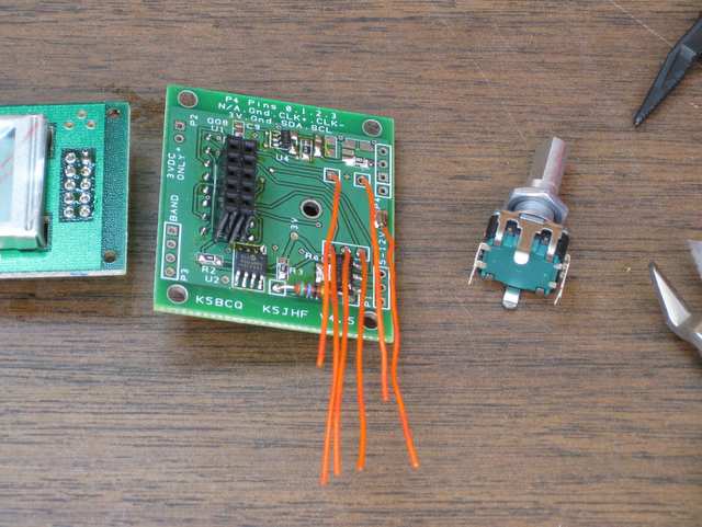
When he came downstairs, I was working on assembling the K5JHF/K5BCQ Si570 synthesizer kit. It turned out to be a bit fiddly, but it is a decent kit. That said, I would not lay out a PCB like this one. It has a number of vias in the middle of pads, and while that’s not a big problem for hand-soldering, I would avoid it in a PCB as a matter of good practice. You never know who might decide to use solder paste and reflow to assemble the board, and then those vias will be trouble.

Worse, though, is the positioning of the connector for the LCD. It is laid out smack in the middle of the footprint for the microcontroller, but on the opposite side of the board. If you look at the big black socket in the picture above, you will see the back side of the microcontroller’s pins poking through the board on either side of it. This positioning means one has to solder the header on one side of the board, then insert the micro on top of the pins one just soldered, flip over the board and solder the micro’s pins next to the header. The header pins are non-serviceable once the microcontroller is installed, and the microcontroller won’t be easy to get out, either. DIP desoldering tools won’t fit with the header in the way. I’m not sure why the board is laid out this way, except that it makes the board a little smaller. Maybe that was the only concern.
At this point, it’s fully assembled except for the encoder/switch, which is about half wired. What am I doing blogging? I could be soldering!