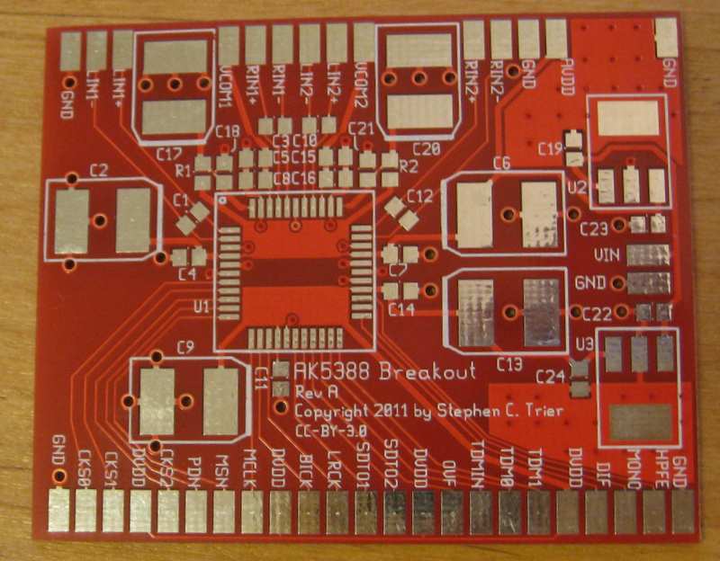
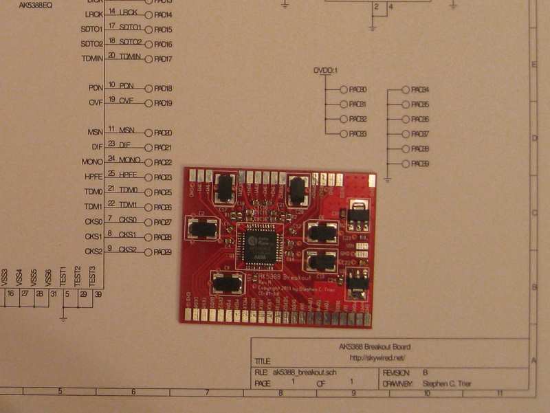
The boards I ordered last month from Itead Studio arrived with something extra: someone else’s boards! No, it was not a mistake, but a 10-cent option that I could not resist: the Open PCB service. For 10 cents above the cost of a prototype PCB order, Itead fabbed two extra boards of my design. Those boards went into a pool of boards from the other Open PCB participants, then Itead sent each of us two random boards from the pool. All participating boards are supposed to be open source. Sure, there is no guarantee that the boards will be at all useful to the recipient, but who knows, maybe something nifty will arrive!
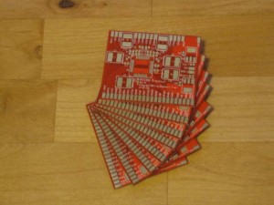
I ordered the Open PCB option with my AK5388 ADC board. Along with my 8 copies of the board, I received two boards from strangers. Both are 5 cm x 5 cm, which is likely a popular size for Itead because it’s the maximum size for their cheapest PCB fab deals.
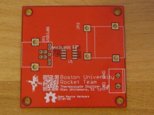
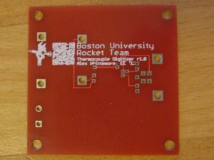
The first board is a thermocouple digitizer from the Boston University Rocket Team. The team has posted the schematics, layout, and Gerbers online on GitHub. The board was clearly labelled, making it easy to find the documentation in Google. It even had a QR code. though the pixels were blurred by the silkscreen and my phone was unable to read it. It’s a great idea for open source hardware, though, and would probably work if it were a little bigger.
The design uses a single MAX31855 as a thermocouple-to-digital converter. This is a neat chip that contains a thermocouple amplifier, cold-junction compensation, and a 14-bit ADC all in an 8-pin SOIC. That’s a ton of analog circuitry condensed into a single chip! It can cover temperatures from near absolute zero to molten metal, with quite respectable accuracy and resolution. The board runs the chip’s Serial Peripheral Interface (SPI) to a USB 3 connector, wired in a non-standard way that carries power (12V, 5V, and 3.3V) and an SPI bus.
The Rocket Team has chosen an interesting mission. They don’t fly rockets, but rather research the design and performance of hybrid rocket motors, including firing them on a static test stand. They build their own instrumentation, all open source hardware, and this board is part of that package. I can see why they would be interested in accurately measuing the temperature of very cold and very hot things!
The board actually has some potential to be useful to me. I don’t need a thermocouple interface right now, but I can imagine using for one down the road to monitor a reflow oven or to manage the heatsink temperature in a linear amp.
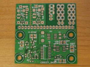
The second board is a bit of a mystery.
On first inspection, I was puzzled by the single-row header right across the middle and the smaller row of holes at the upper-left side. Eventually I noticed that there are no traces running to either, so it’s likely that they are perforations to simplify cutting the board into three pieces.
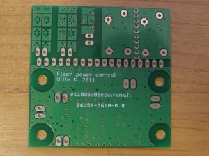
The bottom portion is the least obscure. It bears the labels “Flash power control” and “X-SYNC”, so it must have something to do with photo flash. Beyond that, I’m stumped. A two-pin header for an IGBT (a three-terminal device) particularly leaves me scratching my head. The designer did a nice job of bonding his top-side ground pour to the bottom-side ground plane with plenty of vias, including all around the edge of the board.
On the upper right, there are two copies of a circuit, separated by a row of holes to aid breaking them apart. The circuit has a transistor in SOT-23, a diode, a few capacitors, a resistor, and what is likely an IC in a small 5-pin package. Looking at the topology, I think the circuit is a boost converter, at least if the unlabeled two-pad component on the center left is an inductor.
The patterns in the upper right corner are even harder to understand. They look like series chains of something, maybe resistors or LEDs. The vias in the pads and the wide traces indicate that the designer was concerned about resistance, inductance, or heat dissipation. Since the three-device chain (upper center of the board) has the triple vias to back-side copper, but does not use the copper to interconnect, I would guess heat sinking is the concern. It could be a challenge to reflow the board with the open vias in the pads, but it’s probably meant to be hand-soldered. When hand-soldering, one can keep feeding solder until the holes have wicked up their fill.
I sent some e-mail to the address in the silkscreen but got no reply. Google searches on other likely terms turned up nothing. I’m left with a board and guesses.
The Open PCB exchange is a great idea, and I’ll happily participate again in the future. The thermocouple board is an example of how it can go right. I got a well-documented board that led me to find out about the Rocket Team’s interesting work. In contrast, the Flash Power Control board is an example of what can go wrong. There is nothing to stop someone from entering an undocumented PCB in the exchange, getting documented and interesting boards but failing to repay the favor. Still, I like seeing what other people are doing and hopefully two other people enjoyed seeing what I’m up to. For 10 cents, less than a 1% increment on the cost of a PCB order, it’s worth it.
Have you tried Open PCB, and how did it work out? Are you able to shed any light on the mystery board? As always, comments are welcome!
 “Honey, the package you’ve been waiting for from Hong Kong is by your computer,” said my dear wife shortly after I got home from work on Friday. Even better, a few minutes later she suggested that I spend the evening in the basement, building up one of my new boards. I have a wonderful wife!