Yay! Now we’re getting somewhere!
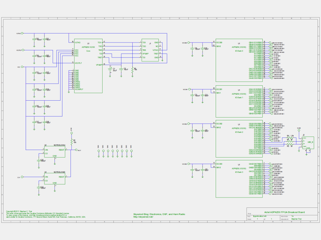
Here is the schematic for the FPGA breakout board.
(PDF: fpga-adapter.pdf)
Most of the schematic simply brings pins to pads for soldering. My intent is that the pads will be arranged around the perimeter of the top side of the PCB, for easy access.
As planned, I committed three pins to USB, with the three resistors required and a USB Type B connector.
The design includes two reset supervisors (U2 and U3). One covers the FPGA core, and the second is uncommitted. The A3PN250 FPGA (datasheet) can take up to seven independent power supply voltages. First, it needs 1.5V to run its core. In addition, each of the four banks of I/O pins has its own power-supply pins and can run at a different voltage. The on-board PLL has its own power supply. Finally, the JTAG interface used for programming the FPGA has its own power-supply pin, so the JTAG interface can run at whatever voltage is convenient for programming without constraining the other I/O voltages. With all of those power supplies, one might think the adapter should have seven supervisors. However, the minimum number is two: One supervisor for the core, and one for the I/O bank that has the reset input. After all, it doesn’t do any good to try to reset the core if the I/O bank isn’t ready to listen! If it turns out we need more reset supervisors, they will be easy to skywire in later.
The two reset supervisors have open-drain outputs, which are wire-OR’ed together so that either supervisor can hold the reset output low. That way, reset will not be released until both the core and I/O power supplies are ready.
For the core supervisor, I used a part with a 1.4V threshold. For the I/O supervisor, I pencilled in a 3.0V part, because I already know the USB interface will need a 3.3V supply. However, another part could be dropped in if I need to wire the reset input to an I/O bank with a different power supply. The supervisor I chose, the ON Semiconductor NCP303 family (datasheet), comes in versions from 0.9 to 4.9 volts, in 0.1 V steps, so there are plenty of options.
Power supply decoupling is important to keep noise down, and doubly so for an RF design. I included a pair of decoupling capacitors for every power supply input.
Finally, the schematic shows plenty of ground pads, eight in total. The board will be designed to sit on a copperclad board, so short wires bonding the ground pads to its carrier will secure the adapter mechanically as well as providing a good RF ground.
I chose parts that are all available from Mouser. I’m usually a Digikey guy, but Digikey doesn’t carry Actel FPGAs. It’s nice to be able to get all the parts with a single order, and besides, Mouser has a better selection of voltages for the NCP303 supervisors.
That’s the design. Next up: the PCB layout!
(UPDATE 4/6/2011: Added Creative Commons Attribution 3.0 license to the schematic.)
