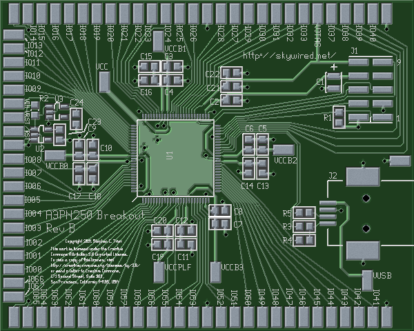
Here at last is the printed circuit board layout for the FPGA breakout board. I’m planning a series of projects involving FPGA-based DSP for ham radio, and in order to build them, I need an FPGA and a PCB on which to mount it. In the last installment of the project, I presented the schematic for the breakout board.
The goals for this layout constrained it to be a nearly single-sided layout, with a ground plane on the back. That way, the board could be mounted directly on a piece of copperclad with no short circuits to ground. My budget limited me to a double-sided board, so all signal and power traces had to go on the top side.
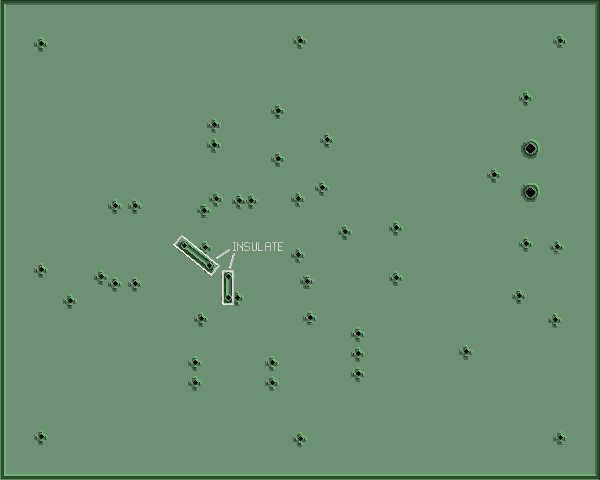
That said, here is the layout, top and bottom.


As you can see, I didn’t quite hit my goal of having all traces on the top side. In order to get power to all of the A3PN250 FPGA’s VCC pins without long and circuitous traces, I had to put two cross-unders on the bottom of the PCB. I’ll insulate them with a bit of Kapton tape. Since solder mask isn’t really guaranteed to completely cover vias, particularly for the cheapest PCB processes such as I’m using here, leaving those traces uninsulated would cause a small chance of a short between VCC and the copperclad ground plane on which this board will be placed.
Another trade-off in the design was the need to keep the decoupling capacitors close to the FPGA, without interfering with the fanout of the signal pins. The placement here was done by eyeball, but it turned out to be not too far off.
Surprisingly, one of the slowest parts of the layout was figuring out which three FPGA pins were ideal for the USB interface. As it stands now, the differential pair (which can be seen sneaking past VCCB2 to R3 and R5) has a bit of a circuitous path, but I think the layout will be adequate. Were I to redo the layout, I would move terminating resistors R3 and R5 closer to the FPGA.
I sent the layout to the Dorkbot PDX PCB Order for fabrication. Laen, who runs the service, is very friendly and easy to work with. The service is cheap at $5/sq. in., and you get three copies of the board for that price. The boards went out in the February 7 panel, and should be arriving here in Ohio around February 26. I haven’t tried the service before, so I’m looking forward to seeing the boards and checking their quality.
I will eventually post Gerbers for the PCB, but first I have to read up on open hardware licenses and pick one I like.
The parts for the boards arrived from Mouser last week. If UPS cooperates, my next post will be with the boards in hand.
(UPDATE 4/6/2011: Added Creative Commons Attribution 3.0 license to PCB layout.)