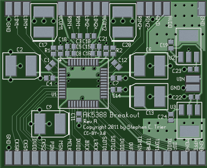
I had some time to myself this weekend and was able to get the AK5388 breakout board routed. The board carries an AKM AK5388 audio DAC, which has 24-bit output and up to a 123 dB signal-to-noise ratio. My plan is to build up this board, evaluate it to verify that it works as I expect, then use it as the ADC stage in a DSP-based ham radio receiver.
Moving the schematic from gschem to PCB was really easy. This was my first time using PCB’s “Import schematics” command. It was a breeze, especially compared to the old way of doing it, the gsch2pcb command. That command worked well enough, but I could never get it done without checking the documentation or a howto online. “Import Schematics” required no such thing. Bravo to the PCB developers!
As with the FPGA board, I laid out the board with a solid groundplane on the back and all components and traces on the front. That way, it can be placed on a piece of copperclad board, for skywired construction, without risk of shorts to ground. It’s also good for noise performance.

The square chip in the middle (QFP, U1) is the AK5388. On the right edge are a 7833 and a 7805 voltage regulator, for the digital and analog power supplies, respectively. The board includes some heatsink area around the regulators (U2 and U3), with thermal vias to stitch the heatsink to the groundplane on the back. The rest of the components are decoupling capacitors, lots of decoupling capacitors, plus two resistors that also help control noise. A 24-bit ADC needs quiet power supplies!
As you might expect, the bottom side is kind of boring:

That’s the ADC board so far. Although I have Gerber files now and could go order the boards, I’m going to order the parts first this time and test-fit them on a printout of the layout.