A few weeks ago, I picked the AKM Semiconductor AK5388 as the analog-to-digital converter for my receiver design. This high-performance audio DAC has a 24-bit output with up to 123 dB signal-to-noise ratio (A-weighted). I hope that the narrower bandwidths of a communications receiver will beat that. The idea is to do the automatic gain control (AGC) in digital, so that the receiver will not need an analog AGC loop. I hope that a preamp or attenuator at the front end will be enough to make up for the limited dynamic range of the AGC.
Now, I am aware that getting performance like that requires great care in the details of the design and layout, but if this wasn’t a challenge, it wouldn’t be nearly as much fun! The AK5388 datasheet does give me some concern, because it does not make much mention of the techniques needed for a high-performance DAC. Admittedly, datasheets from Japanese manufacturers are often thinner on details than those from the leading US suppliers, and this one is much more complete than some. On the other hand, it may be that the datasheet is glossing over any coddling this chip will need.
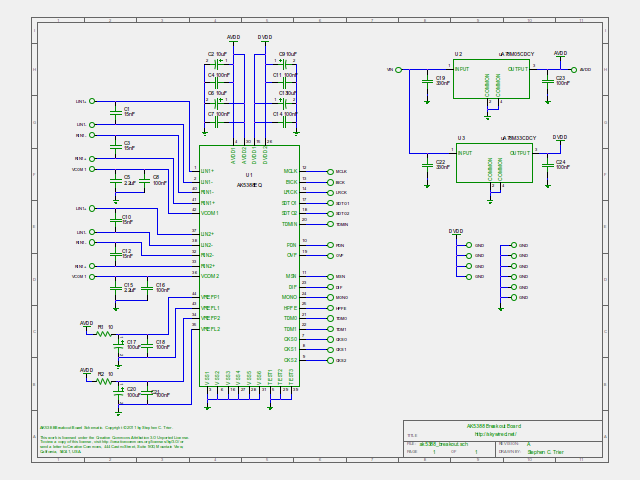
There is one way to find out, and that is to start breadboarding. This is a surface-mount part, so I have designed a breakout board very much like the board I built for the Actel Microsemi A3PN250 FPGA. The schematic is below.
The schematic largely follows the “System Design” section of the datasheet and the example of the AKD5388-A evaluation kit (PDF). It’s not strictly a breakout because I included on-board analog and digital power supplies. An ADC like this needs quiet, local power, so I picked some reasonably quiet supplies and put them on-board. I chose 7800-family regulators from TI because they have reasonable noise specifications. I almost went with other choices that were explicitly designed for low noise, but they were quite a bit more expensive for not much less noise. The AKD5388-A kit uses an uA78M05 and claims to be able to obtain the full dynamic range of this ADC, so there is little reason to spend more at this point.
I’m using the analog power supply as the voltage reference. I considered a dedicated reference, which would be more expensive but perhaps lower noise. Here, too, I followed the lead of the evaluation kit.
The PCB layout should be straightforward. I like to build by skywiring components over a groundplane, so this breakout board will be designed to sit directly on a groundplane, with all components and connections on the top side. All external wiring points will be pads on the PCB, ready for soldering, just as with the A3PN250 FPGA board.
I’m excited about trying out this part. What do you think? Comments welcome!
