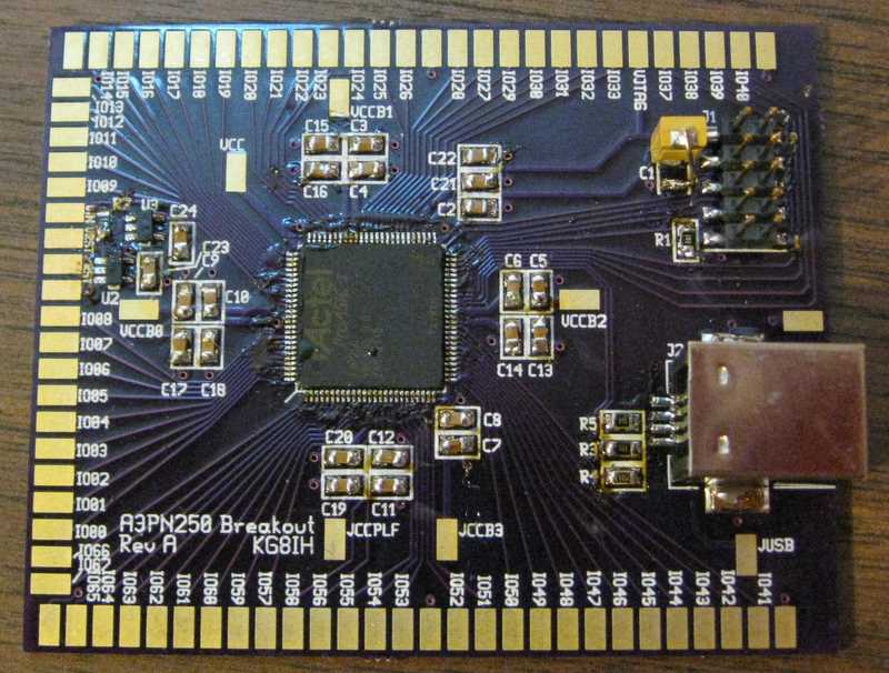
I’ve recovered from the busy last few months and that means I can spend a little more time at my workbench. The first of the A3PN250 (ProASIC3 nano) FPGA breakout boards is built. Here it is, in all its glory:

There is a fair bit of flux residue left on the board. I’ve ordered some flux cleaner and isopropyl alcohol for cleaning it up. While I was at it, I ordered a replacement FPGA for the second board. I knocked its pins out of position while soldering it, and in the course of unsoldering it, not all the pins survived. That happens with these QFP packages. At least it was only $10. Those goodies should arrive early next week.
I had hoped to power up the board for the first time, but thought I should scan the pins for shorts first. This being a breakout board, that process was a simple matter of walking a pair of multimeter probes down the pads, with the meter set to beep for low resistance. I found about a half a dozen shorts, including two shorts from power to ground.
The shorts were easy enough to clean up with a bit of solder wick. Two had the shorting solder behind the pins, where the wick couldn’t reach. For those, I used the counter-intuitive approach of adding more solder, making the short worse. The bigger blob could be touched by the solder wick, and its capillary action easily sucked up the larger solder blob.
I’ve found two errors in the PCB so far.
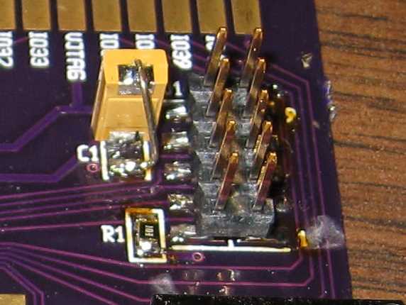
First off, the C1 footprint is much too small. I’m going to have to dig a little to figure out what happened there. Did I use the wrong footprint or buy the wrong part, or was the footprint wrong? In any event, it was easy enough to work around by standing C1 on end on one pad, with a bit of wire to tie it to the other one. This capacitor is the power-entry filter for one of the programming voltages, for which there are more decoupling caps closer to the FPGA, so I am fairly sure the extra inductance will not cause a problem.

The second error is next door to the C1 problem, and it will be harder to deal with. J1, which is the 10-pin JTAG header used for programming the FPGA, has the pins all scrambled. It turns out I accidentally used a footprint that had IC-style numbering instead of one with ribbon cable-style numbering. Unfortunately, the JTAG connection runs over ribbon cable, so all but pin 1 are wrong. I will be working around this one by building a custom ribbon cable that unscrambles the connections. It will cost all of $3.50 plus a bit of time wrangling the wires.
I will add a note to the project page to warn anyone who might want to build a few of these boards.
That’s all for this week. Next week’s jobs will be to clean up that ugly flux and to build the modified JTAG cable so I can bring up the board. Stay tuned!
UPDATE 4-DEC-2011: Yi Zhou reports that C1 should be a 0.33 μF cap, not 33 μF, and that an 0.33 μF cap in an 0805 package fits the C1 footprint. Thanks for catching the error and suggesting the 0805, Yi.