I’m slowly making progress on my KK7B R2/T2 transceiver project. At my last report, I was waiting for replacement capacitors to arrive. They did, and I pulled out my ancient solder-removal iron, a Radio Shack unit from who knows how long ago.
Either my unsoldering skills are rusty or I was too impatient, or both. I managed to lift four pads, completely demolishing one. The other three were salvageable. I’d like the board to be perfect, but having it work is an acceptable substitute.
The new caps went in easily, with only a little fiddling to wire around the ruined pad. Better yet, the excessive bias current I saw before the replacement is gone! The board is supposed to be adjusted to 100 mA current. It used to start at 120 mA, with the bias adjustment set to its minimum, and drift its way up to more and more current from there (going as high as 200 mA before I’ve lost my nerve and switched it off). Now it starts at 84 mA and… drifts its way up from there to 130 mA and more.
OK, so one problem was solved. I can always increase current with the bias adjustment potentiometer.
After scratching my head a bit, I finally noticed one small sentence in KK7B’s articles on the R1 and R2. The audio output transistors need a heat sink, do they? Oops! I dug around a bit in my junk box but couldn’t find anything that would fit. The articles say the audio amp will drive a pair of headphones fine without the output transistors, so I decided to take them out.
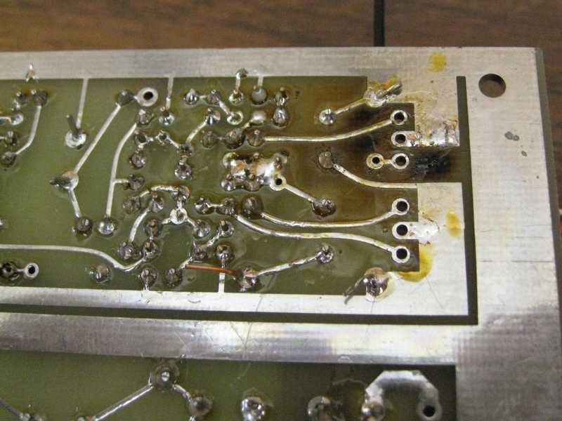
I recently got a Sparkfun hot-air soldering station (a Sparkfun Free Day prize!) and thought I’d give it a shot. Sure, hot air is usually for surface-mount parts, but solder is solder, right? Not being sure how to set the airflow and temperature settings, I set both on the high side, put some flux on the output transistors’ pads, and went for it. The result wasn’t pretty:

Yes, I scorched the board. Oops. Between this and the lifted pads, I think I need to work on my unsoldering skills.
Since the transistors are 50 cent parts (TIP29/TIP30), I unsoldered them the easy way: I cut the leads, removed the leads from the board with my conventional iron, then cleaned out the holes with my solder sucker. I didn’t damage any pads this time! (The picture above was taken after all of these steps.)
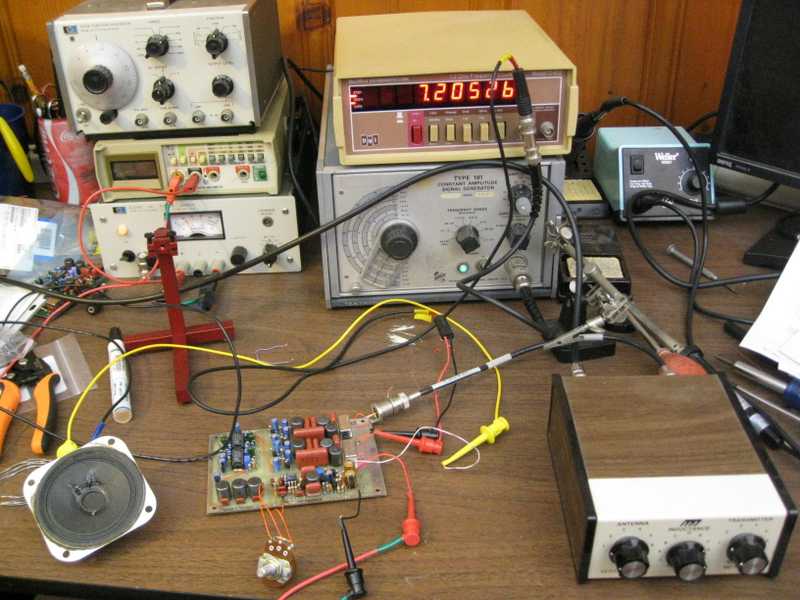
A little more soldering to hook up a BNC and some other goodies, and the board was alive!

That’s a Tek 191 signal generator as the VFO (variable frequency oscillator), with a frequency counter as the readout. That’s an MFJ QRP antenna tuner in the foreground.
I didn’t build a phasing network yet, so I drove only one VFO input. That causes the R2 to function like a conventional direct-conversion receiver,receiving both sidebands simultaneously. That said, it works. I was able to hear signals, though frankly many were quite hard to copy. I’m not sure what else might be wrong.
The frequency counter spits out a lot of digital noise. I learned to flip it on only to spot-check my frequency. It’s a lot quieter in standby mode.
Did I mention that IT WORKS?
Despite the success, I’ve been struck by a bit of paralysis in moving forward. There are so many choices to make for integrating the radio.
- What kind of VFO should I use? Should I design my own or buy a kit?
- Which modes should I include?
- How much power output do I want?
- What power amp should I use? Should I design my own or buy a kit?
- Which case should all of this go in?
- What microphone, and microphone connector, should I plan for?
Keep in mind that this is supposed to me my fast route to getting on the air, so I’m thinking kits for both the VFO and amp. Besides, with as busy as it has been at work lately, it is nice to sit back and just build something.
It’s not a pretty project any more, but it works! Hooray!
Hello Stephen,
I’ve had similar anguish to finishing my R2 receiver as you seem to have 🙂
Bought my R2 kit from KangaUS in 1995 and actually completed building the kit only a few days after receiving it. It was not until august last year that I finally finished building a VFO for it though, so wasn’t able to test its function or performance until then.
You can listen to it in this video clip:
http://www.youtube.com/watch?v=osKlonSWavk&feature=youtu.be
Since I recorded the video the VFO now is modified to cover only half the tuning range as seen in the clip (now tuning only 14000-14055 kHz).
From the beginning I was planning for my receiver to cover the CW portion of the 20mb, but never seemed to ramp up the currage to build the VFO. Despite the fact that I had gathered all the needed parts. I even bought and modified a HW-8 so that I could use its VFO and replace the internal DC receiver with my R2 board. That never happened. Sold the HW-8 before I got to try the idea.
Just now I’m listening to my R2 receiver and it’s a real joy to hear the sounds comming out of it. The opposite sideband rejection is not really to my satisfaction though. I’ve measured it to be 39 dB and that is about what to expect from the design. So that’s ok, but on the band when tuning in stations stronger than S9 they can also be quite readable in the suppressed sideband. If you look closely in the video you can see some strong stations tuning in the opposite direction to other weaker stations 🙂
Now I’m really eager to try out the R2Pro. That design will hopefully help me achieve more than 50 dB of opposite sideband rejection.
Ultimately I would also like to try out a DDS VFO for these phasing type DC receivers. I’m thinking of a pair of AD9951’s… maybe controlled by an AVR32…
Alrigh, keep up the good work Stephen. Hope to see more info on the progress of your projects here on the blog soon.
Be seing you.
Regards,
Patrik
SM7NWJ