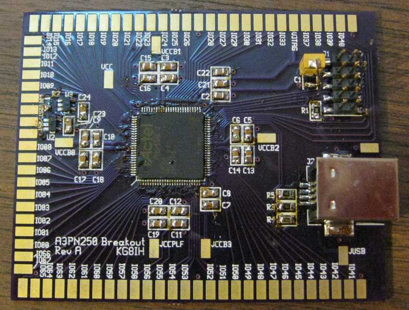
I’ve recovered from the busy last few months and that means I can spend a little more time at my workbench. The first of the A3PN250 (ProASIC3 nano) FPGA breakout boards is built. Here it is, in all its glory:

Exploring the space where hardware and software meet
I’ve recovered from the busy last few months and that means I can spend a little more time at my workbench. The first of the A3PN250 (ProASIC3 nano) FPGA breakout boards is built. Here it is, in all its glory:

This is too neat not to share: How to solder through-hole parts, as a one-page comic, by Mitch Altman and Andie Nordgren.
Soldering Is Easy (via MightyOhm)
I’m happy to announce a new tutorials section here on Skywired! A click on “Tutorials” on the menu bar above will take you to a list of Skywired’s how-tos and explanations. The first tutorial is about how to solder fine-pitch parts, such as QFPs, TSSOPs, SOICs, and so forth. Over time, I plan to expand the range of tutorials to cover both practice and theory.
After a busy week spent traveling for work and a morning digging out from a surprise snowstorm, I had a great weekend with my family. It was Sunday night before I heated up the soldering iron and got down to business building the ProASIC 3 nano FPGA board.
I started with the toughest component, the FPGA. Its central location and low height means ….
After a busy week spent traveling for work and a morning digging out from a surprise snowstorm, I had a great weekend with my family. It was Sunday night before I heated up the soldering iron and got down to business building the ProASIC 3 nano FPGA board.
I started with the toughest component, the FPGA. Its central location and low height means that I will have an easier time accessing it before other components are mounted. That is not likely to be a big problem for this board, with plenty of space around the chip, but I would still prefer not to have to work around the filter capacitors if I can avoid it. On the other hand, its 100 pins and 0.5 mm pin pitch makes it far and away the most difficult soldering job on the PCB.