PCB layout is fun, especially when you are trying to eke the best performance out of a component. Last week, I finished the PCB layout for the AK5388 analog-to-digital converter (ADC) I chose for my digital ham radio transceiver project. Let’s take a closer look at some of the design details…
My top priority was to keep digital lines away from sensitive analog signals. The quickly-switching edges of digital signals carry lots of high-frequency components, which readily couple into any neighboring line. It’s best to keep this high-frequency crud away from quiet analog signals. It’s not great to let it couple instead into other digital lines, but digital inputs are pretty tolerant to it and rarely have problems.

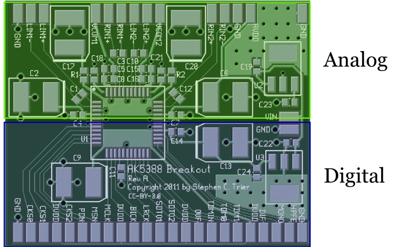
The AK5388 pinout helps a lot with this separation requirement. As is done in many ADCs, all of the digital pins are on one side of the chip, and all of the analog pins on the other. When laying out a mixed-signal board (that is, one that has both analog and digital elements), I like to draw a line across the board before I even start to place the parts, with all analog components going on one side and all digital on the other. As the placement and routing progress, that line will move and may even change into a zig-zag, but the idea remains: Keep the analog stuff on one side and the digital on the other.
On the AK5388 breakout board, the analog-digital border remains a straight line. Everything in the top half of the board is analog, and everything in the bottom half is digital.
Another reason to have a clean split is the return currents and their IR drop. Remember that current flows in a loop. When any of those digital lines changes state, it charges a small capacitance at the other end, and the current used to do that charging flows back through the ground plane. At high frequencies, that return current is largely confined beneath the digital line that caused it. On top of that, the return current causes a voltage gradient underneath it, thanks to Ohm’s law and the resistance of ground. (V = IR) This voltage gradient can act as an additive noise source on analog signals that are routed near it. The careful split in this board’s design will help keep the digital return currents from affecting the analog signals.
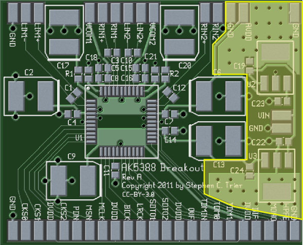
Another feature of the board is that it has local analog and digital power supplies for the ADC. The power supplies are located in their own area, again to try to limit noise caused by the return currents. In the picture below, the power supplies are highlighted in yellow.

The voltage regulators used here (uA78M33CDCY and uA78M05CDCY) are in SOT-233 packages, which have a large lead on one side to help with heatsinking. The board is laid out with some extra copper area to act as a heat spreader for each SOT-223, along with a bunch of vias tying the top-side copper to the ground plane. These vias have a thermal role, not primarily an electrical one, as they help transfer heat from the top-side heat spreader down to the ground plane to further spread it out.
Although there are ways to estimate the thermal performance of a heat-spreader design like this, I didn’t do them. Frankly, I don’t have any idea whether this board’s thermal provisions are adequate. Even at the bargain price of $5/square inch to have this PCB fabbed, adding copper just for thermal management gets expensive. If the heat-spreading area turns out to be insufficient, I’ll find a way to attach a heatsink to the top side of the regulators, solder a piece of brass to their large lead, or something along those lines to remove the heat more efficiently.
Finally, take a look at the decoupling capacitors. C4, C7, C11, and C14 are 100 nF capacitors, each on one power-supply input to the ADC. They are positioned as close to the ADC as I could manage. One could argue that their positioning is not quite perfect because there is a relatively long path from their grounded side to the closest ADC ground pin. It goes through two vias and the ground plane. I have never looked into whether this makes a significant difference. If you know, leave a note in the comments and tell me!
In any case, the 100 nF capacitors are multi-layer ceramic capacitors (MLCC), which have a low equivalent series resistance (ESR) and inductance (ESL). Those characteristics make them ideal for decoupling high-frequency noise on the power supply lines.
Next, C2, C9, C22, and C23 are big 10 μF decoupling capacitors. These are positioned a little farther away. They are aluminum electrolytic capacitors, which have a higher ESR and ESL than ceramic caps. (10 μF ceramic capacitors are expensive!) These capacitors are better for removing low frequencies, including the audio range, from the power supplies. For that reason, I did not see much harm in putting them a little farther from the ADC, with the extra inductance and resistance that implies. Besides, these things are BIG! If they were any closer to the ADC, routing the signal lines in and out would get pretty challenging.
One trick for getting the decoupling capacitors closer is to put them on the back side of the board. The distance through a via would be much shorter than the distance needed here. I wanted a single-sided design here, so that wasn’t an option, but it’s something to keep in mind.
I won’t claim that I know everything about designing for a high-performance ADC. In fact, it’s possible that someone more experienced is planting their face in their palm right now, saying, “I can’t believe he did that!” (If that’s you, by the way, drop me a note to let me know what the problem is, would you?) That said, what I did here is based on app notes and other materials from a number of semiconductor companies, including Analog Devices and National Semiconductor, and I think it’s pretty sound.
I ordered the parts for this board today. It doesn’t take long for UPS to get things to Ohio from Digi-Key’s home in northernmost Minnesota, but it’s always a long wait when I’m itching to try something out.
I’ll catch you next week with more on electronics, DSP, and ham radio.
Thanks for the long explanation of everything that you did. I’m studying as an electrical engineer and all the knowledge you are sharing really helps me out.
Thanks again
Dillon
Dillon,
Thanks for the kind words, and I’m glad you like my rambling discourses. It looks like you’re having fun with some interesting projects, too. Keep in touch!
Stephen
P.S. Sorry about the delay in posting. Your comment got caught in the spam filter, and it took a while for me to find it in there.
Hi Mr. Trier,
I’d like to license one of your PCB layouts. Could you please reply to my email so I can discuss with you further? jerryzy yahoo.com
Thanks!
Yi
Hi, Yi.
Both of the layouts posted so far are licensed under the Creative Commons Attribution 3.0 license. That means you already have a license to share the work, to adapt it, and/or to use it commercially. The only major requirement I impose is for you to attribute the work to me. See the license summary for more information.
I am willing to license the designs under other terms. If Creative Commons does not work for you, please send me e-mail at sct@skywired.net so we can discuss.
Stephen