Hi, I’m back! It was a rough week, with a death in the family. As it ended, I found some time for some “solder therapy”. There is something good for the soul in putting together electronics. I don’t know if it’s the scent of the rosin or the satisfaction of seeing a project come together. All I know is it’s good for me.

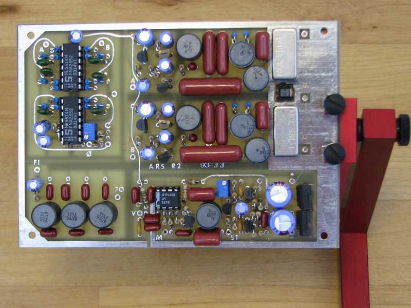
The target of my soldering was my KK7B R2 receiver kit. This is the companion to the T2 I wrote about a few weeks ago. To my surprise, the R2 was easier to put together despite the higher part count. The components are larger, forcing a less dense pin matrix, and the board is separated into sections: mixers and diplexers, audio phase shift, low-pass filter, and audio amplifier. Conveniently, the board uses jumper wires (not yet installed on mine) to connect the sections. The intent appears to have been to make it easier to extend the board by swapping in a different phase shift network or adding alternate filters for CW or contesting, but it will make the board easier to debug as well, since I can bring it up a section at a time.
Keep in mind that this is a vintage kit that is no longer available, but updated versions of the design are still produced by Kanga US.
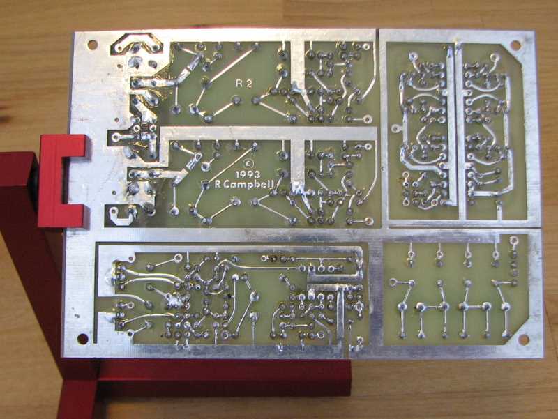
The board surprised me with its heft. I work mostly with surface-mount digital boards where the fiberglass PCB is the heaviest component. This board, though, weighs 134 g (4.7 oz), which is a lot for 100 cm2 (16 in2). The shielded inductors are the culprits. Each black cylinder in the photo is the ferrite shield of an inductor. Each inductor is noticeably heavy for its size, and this board has 10 of them.

Once I wash the flux off (it’s not as much fun as soldering), the next piece of the puzzle is to build or buy a VFO. Rick, KK7B, designed a companion VFO for these boards, but it is out of production at the moment. I’m thinking about one of the Si570 VFOs out there. This little chip offers a very low phase noise synthesizer with tuning in steps of a fraction of a Hertz. Having this on a single chip was a pipe dream when the R2 and T2 were designed.
After that, I’ll need to build a power amplifier to boost the T2’s milliwatts up to a reasonable level — at least a watt, maybe as much as 50 W. Finally, I will have to integrate all the pieces into a working rig. Professionally, I do a lot of microcontroller work, so it’s tempting to build a fancy digital control panel with circuitry to integrate every R2 and T2 option imaginable. Instead, I’m trying to keep myself to something simple: one band, SSB only, and a digital frequency readout as the only frill.
I still have to pick the initial band. I’m torn between 20m, my favorite for PSK31, and 40m, which I like for SSB. I’m after whatever DX I can land in either mode. What band would you recommend?