This post is part of a series on delta-sigma techniques: analog-to-digital and digital-to-analog converters, modulators, and more. A complete list of posts in the series are in the How Delta-Sigma Works tutorial page.
Today I’d like to turn to the fascinating topic of delta-sigma techniques. Delta-sigma is best known for its use in analog-to-digital and digital-to-analog converters, but it also has a potent role in digital signal processing and even in analog applications. By its nature, delta-sigma can reduce the amount of analog circuitry needed in a radio or other electronics, and what is left is often simpler and cheaper than what would otherwise be required.
Beyond that, delta-sigma techniques are nifty! The core concept is counter-intuitive at first glance, yet it offers all kinds of powerful applications. Working at understanding delta-sigma techniques gives deep insights to many other areas of signal processing.
This is the first of a multi-part series on delta-sigma, which is too broad and deep a topic to cover in a single post. There will be some math, balanced with an intuitive approach to the circuits. I will also delve into the the practical, building delta-sigma data converters and sharing the schematics and results. I will be learning about delta-sigma along with you, so stay tuned for more in future posts.
The place to begin is with a first order delta-sigma modulator, which is the simplest variety of delta-sigma circuit. A first-order modulator has a structure like this:
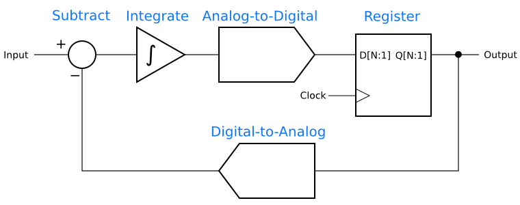
It turns out that delta-sigma techniques do not require many bits in the ADC and DAC. In fact, many applications need only a one-bit ADC and DAC. A single-bit ADC is just a comparator, and a single-bit DAC is a transition between the digital and analog domains for a signal. Depending on the implementation details, it might reduce to nothing at all, or there might be some actual DAC circuitry.
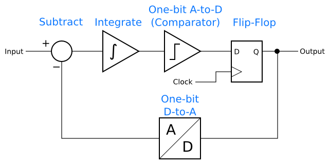
Since we are in the world of theory at this point, assume that our input signal is between 0 and 1 and the digital signals are either 0 or 1. To keep things really simple, assume that a digital input acts like a comparator, reading any value about 0.5 as a logical “1” and reading any value below 0.5 as a logical “0”. This isn’t entirely unrealistic — it’s basically an idealized version of CMOS logic.
With those assumptions, the circuit becomes even simpler. There is no longer a need for a comparator, because a logic input can handle the job, and there is no need for a DAC, because the logic levels are compatible with the analog levels.
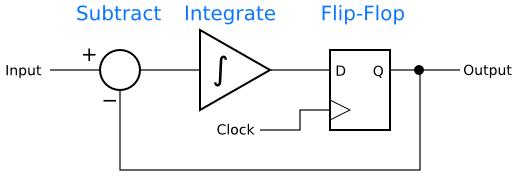
For one last assumption, let us say that the integrator as a time constant of 1 period of the clock input. That is to say, an input of 1 to the integrator for 1 clock input will cause the integrator’s output to increase by 1.
Suppose the input to the circuit is 0.6, the integrator’s output is 0, and the output of the flip-flip is 0. The sum will be (0.6 – 0) = 0.6. One clock cycle later, the input to the flip-flop will be 0.6, which is above 0.5, so the flip-flop will output 1. The sum will now be (0.6 – 1) = -0.4. After that is integrated with the previous value of 0.6, the output of the integrator, and input to the flip-flop, is (0.6 + -0.4) = 0.2. That is less than 1, so the flip-flop will output 0.
This process can be shown in table form:
| Sum | Integrator Out | Flip-flop new output |
| ⋮ | ⋮ | ⋮ |
The integrator output quickly settles into the sequence {0.6, 0.2, 0.8, 0.4, 1.0, …}, and that leads the flip-flop output to follow the sequence {1, 0, 1, 0, 1, …}. In other words, there is a limit cycle causing the output to have a repeating pattern.
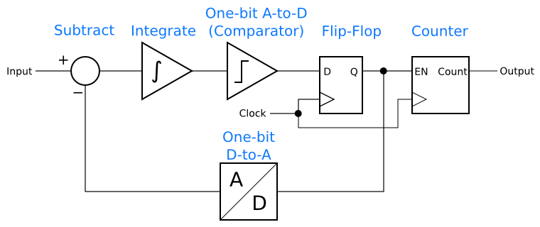
This pattern has an amazing property. Its average value is equal to the value at the input of the modulator! In this case, three out of every five cycles are 1, for an average of 0.6. It turns out that all inputs in the range (0, 1) will result a binary sequence at the output with an average value equal to the input. This may not look much like the heart of an analog-to-digital converter, but it is. All that is needed is a counter to count the number of 1’s in some length of time. The count of 1’s will be proportional to the analog input value.
The same modulator topology has applications in analog-to-digital, digital-to-analog, digital-to-digital, and analog-to-analog applications! If the subtraction and integration are done in analog, and the number of 1’s in the output counted, as described above, one has an analog-to-digital converter.
If one instead has an digital input, the subtraction and integration can be done digitally, with an analog low-pass filter on the output to obtain the average value. That makes a digital-to-analog converter, as shown below.
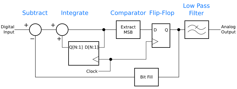
Moving the “front” of the modulator from the analog to the digital domain has caused a few of the blocks to change, but their function is the same. The integrator has been replaced by a digital integrator. The integrator has a loop with a sum block, marked with two “+” plus signs, and a register. The integrator adds its input to the value stored in the register, then on each clock stores the sum in the register. Thus, it works like an analog integrator, adding up the history of its inputs.
Another change is that the comparator was replaced by a block that extracts the most significant bit from the integrator’s output. Assume for the moment that the input to this modulator is four bits wide. A digital equivalent to the analog comparator would output 0 for the binary numbers 0000 to 0111, and would output 1 for the binary numbers 1000 to 1111. Therefore, rather than a full-blown comparator circuit, all that needs to be done is to extract the most significant bit (MSB) of the data word, which is 0 for the lower range and 1 for the upper. This is assuming an unsigned input to the block. Signed numbers using 2’s-complement notation will require the inverse of the MSB.
Finally, a “bit fill” block takes the place of the digital-to-analog converter in the first diagram, above. This block is responsible for extending the one-bit signal back to the full bit width of the input. To accommodate a full range of inputs, the output should be the minimum number for 0 input and the maximum for 1 input. For our 4-bit system mentioned above, with unsigned numbers, the block would output 0000 for a 0 input and 1111 for a 1 input. In other words, it can be as simple as wiring the input bit to all four output bits in parallel.
The block diagram above is quite a bit more complicated than the simpler analog systems shown earlier. It can be simplified in an elegant way. The first step is to recognize that the MSB extraction and the flip-flop can be switched around. The flip-flop needs to be extended into a register that holds a full data word instead of a single bit. Thus, this version, which is shown below, is actually less efficient than the original version. It is a step in the right direction, though, which you will see in just a moment.
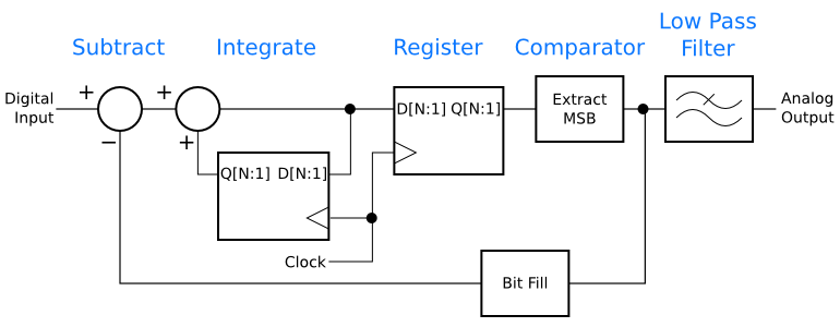 The delta-sigma digital-to-analog converter pictured above has one oddity that is easy to remove. There are two registers shown, one in the main signal path, and the other in the integrator’s feedback loop. Both are storing the same data and are clocked from the same source. By replacing the two with one register, we get the delta-sigma digital-to-analog converter shown below. This is a good, simple delta-sigma D-to-A.
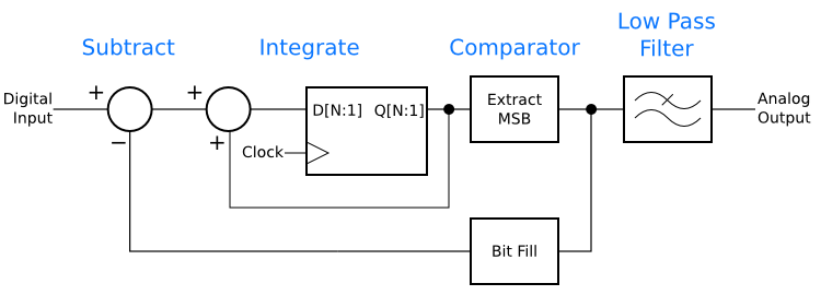
More advanced delta-sigma A-to-Ds and D-to-As have a home in nearly every piece of digital audio gear, not to mention everything from cell phones to personal computers.
Delta-sigma modulators have digital-to-digital applications as well. The number of bits in a digital signal affects the amount of chip area required to process it, while digital logic is capable of speeds far in excess of the bandwidths we humans can process. One solution is to use a delta-sigma modulator to transform slow, wide data, such as digital audio, into fast, narrow data. One can then process the data on a small, fast chip before running it through a digital low-pass fitler to convert it back into a slower form.
Finally, delta-sigma converters are useful in analog-to-analog applications. Some high-efficiency audio amplifiers are built around delta-sigma modulators, and delta-sigma makes a handy way to transport analog information across an optical isolator.
Optoisolators use an LED and a phototransistor to transmit data across an air gap, which is useful in a variety of systems that need to have separate ground references on each side of the optoisolator. For example, optoisolators are used in many medical devices to protect the patient from line voltage. The drawback to optoisolators is that they are not especially linear, and worse, over time the LED ages and becomes dimmer, reducing the gain across the isolator. Optos, as they are sometimes called, are good for digital data, but can be tricky to use in an analog system.
One solution to the problem is to use a delta-sigma modulator on the transmitting side of the link. The modulator translates the analog signal to a one-bit digital signal, which then drives the optoisolator LED. The phototransistor receives the digital signal, which can be run through a buffer and a low-pass filter to recover a copy of the analog signal.
The first-order delta-sigma modulator is the entry point to a world of fascinating techniques. In truth, few systems use first-order modulators, but understanding the first order is the stepping stone to more sophisticated systems. Coming up in future installments of this series are a look at how delta-sigma modulators simplify analog design, and building a delta-sigma converter on the bench.