How Delta-Sigma Works, part 3: The controls-system perspective

This post is part of a series on delta-sigma techniques: data converters, modulators, and more. A complete list of posts in the series are in the How Delta-Sigma Works tutorial page.

In the first installment of How Delta-Sigma Works, I presented the basic first-order delta-sigma converter loop. Now it is time to begin digging a little deeper and look at how the loop works. To do this, we will need the mathematical tools of closed-loop control systems. Even without the mathematics, thinking about a delta-sigma modulator as a closed-loop controller can bring insight into how it works.

In engineering, closed-loop control is often used to keep a system working at a setpoint despite environmental disturbances or variations in the system itself. A furnace thermostat is a simple closed-loop controller, turning on the heat when the temperature drops below a setpoint and turning it back off when the temperature is above. Another example is vehicle cruise control. Unlike a thermostat, which usually has a binary output (on/off), cruise control adjusts the engine fuel control to maintain a roughly constant speed. In my car, it does this by physically moving the gas pedal. The environmental variations cruise control can encounter include hills, the quality of the fuel, and headwinds or tailwinds. The closed-loop controller adjusts the gas pedal as needed to maintain constant speed despite these effects.

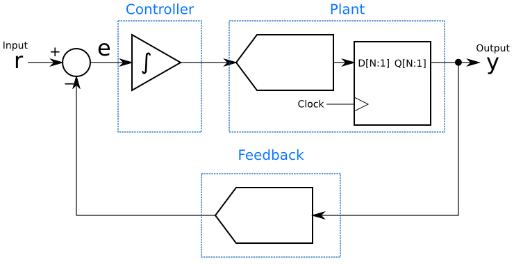
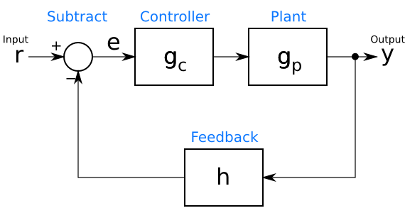
A simple closed-loop control system can be drawn as in the figure below. The reference input, r, is the command input to the controller. In the thermostat example, r is the setpoint temperature, while for cruise control, it is the set speed. The output, y, is the controlled value. This is not necessarily in the same units as the reference input r. For example, in the cruise control, y might be a direct measurement of speed, or it might be something else related, such as a cumulative count of revolutions of the vehicle’s wheels.

Basic closed-loop control system

In between the input r and the output y is the control loop. At the bottom of the loop, in its feedback path, a block h processes the output y into a form that is subtracted from the input r to create an error signal e. This error signal is an indication of how far the controller is from the desired operating point. The goal of a controller design is to keep e near, if not at, 0. The feedback block h can represent many different things. In the example of a cruise control system with the output y in units of distance, h might calculate speed by computing the derivative of y. In other systems, h might simply scale the value to convert its units. If y and r are already in the same units, such as in a thermostat example, h can pass through y unchanged (h = y).

Now that the error signal has been calculated, it is processed by the controller gc, the output of which goes to the “plant” being controlled. (To a controls engineer, anything being controlled, whether a car, a heating system, or a giant factory, is a plant.) The plant is represented by the box gp. The processing in the controller gc is easy to grasp. The controller calculates some function of its input in order to find the command it should give the plant.

What happens in this plant, gp, may be a little harder to imagine. The function gp is a mathematical model of the physics of the actual plant. It may be calculated from basic principles (a physicist’s delight!), or it may be an empirical model derived from the inputs and outputs of the actual plant. In any event, a reasonable guess at the function gp is necessary before one can design a closed-loop controller.

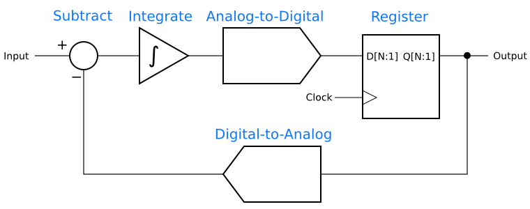
A delta-sigma modulator also has a closed loop, which suggests that perhaps insight can be gained by comparing it to a controller. The first-order delta-sigma analog-to-digital converter from the first installment, is shown again below.

First-order delta-sigma modulator

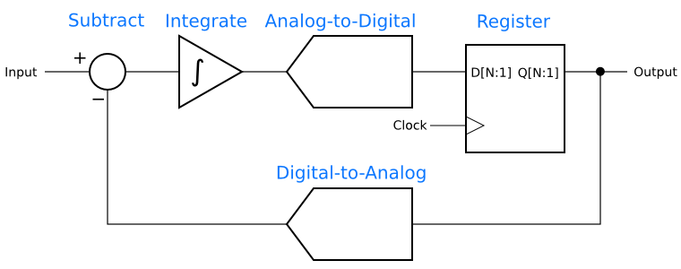
The resemblance to a closed-loop controller is clear when one groups the blocks as in the next figure. The subtractor has the same function in both diagrams, comparing the input to the output. The integrator functions as the controller, gc, and the analog-to-digital convertor and its register are the plant, gp, being controlled. The digital-to-analog converter is the feedback path, h.

Grouping the delta-sigma elements by analogy to the closed-loop controller

This grouping gives immediate insight into how the delta-sigma modulator does its magic: It is a linear controller for an analog-to-digital converter, which is the plant. The controller is always trying to drive that plant’s output as close as possible to the setpoint, and does so by adding up (integrating) the error signal. Also, since the integrator is adding up the history of the error signal, it can be seen that although the output at any given moment may not equal the input, the long-term average will be equal. That integrator will try to keep the long-term average of the error, e, equal to 0.

There are many controllers that can control a given plant. PID (proportional-integral-derivative) controllers are simple and very popular, while more sophisticated controllers can be designed using other techniques. If a delta-sigma modulator is a control loop, it is reasonable to ask if controllers other than an single integrator will result in a better-performing modulator. In fact, other control functions can be used in delta-sigma modulators and can give lower noise or more desirable characteristics in the frequency domain.

Finally, one should not get too carried away with a linear control model. Analog-to-digital and digital-to-analog converters are inherently non-linear, while the mathematics of control theory primarily deals with linear systems. Assuming linear behavior will get us a long way towards understanding delta-sigma techniques, but it is important not to take the analogy too far.

Next in this series: Noise shaping, the frequency-domain secret behind delta-sigma data converters.
Humbled by a sine wave oscillator

The old saw goes, “oscillators don’t, amplifiers do”, but that’s an analog saying.  It doesn’t apply to the digital world.  After all, digital is easy, while analog is hard, right?  (Be careful not to answer too quickly!)

For the last few weeks, I’ve spent my tinkering time on adding sine wave sidetone to the Verilog iambic keyer. As you may recall, sidetone is audio feedback for the keying, in other words, audible Morse code.  My thinking was that while this would appear to be a side trip on the way to FPGA-DSP radio nirvana, it would actually be valuable.  My vision for the radio will require sine wave synthesis in a couple of places.  Also, to have sine wave sidetone, I will need a digital-to-analog converter (DAC), so why not put theory into practice and build a delta-sigma DAC?

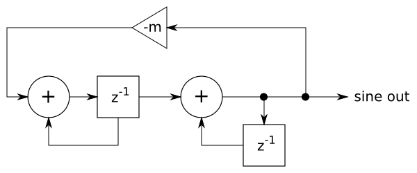
I looked around a bit to find a good way to synthesize a sine wave.  I didn’t want to do a simple ROM lookup table, because the radio will need memories for storing filter data and coefficients.  Instead, I settled on an algorithm that uses two integrators and a multiplier.  For some ratios of clock to output frequencies, the multiplication by -m can be reduced to a simple right-shift, which is always appealing to a hardware designer because it can be implemented without any gates.  The negation can then be absorbed into the first adder, costing little more than a set of inverters and a carry input.

Two-integrator sine wave oscillator

Then I found this elegant topology in Delta-Sigma Modulators: Modelling, Design, and Applications, by Bourdopoulos et al:

Digital sine wave oscillator with delta-sigma feedback

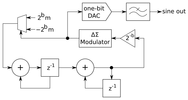
In this design, the multiplier has been replaced by a delta-sigma modulator and two constants.  This is gorgeous!  First of all, the multiplier is gone, replaced by a few adders and a mux.  Secondly, the delta-sigma bitstream is a built-in output for a DAC. There are a couple of wrinkles. First of all, there needs to be a scaling by 2^{-b} before and 2^b after the delta-sigma modulator. Otherwise, the modulator will see signals outside of its stable range. (Stability is a topic for a future tutorial in the How Delta-Sigma Works series.) Second, I’m not sure about putting the delay of the delta-sigma converter into the loop. It seems to me that the two integrators should be non-delaying. Third, are the two integrators sufficient filtering to remove the delta-sigma’s high-frequency noise, or is there a risk of high-frequency feedback making the loop unstable?

It sounds great, but when I coded it up in Verilog I couldn’t get it to be stable.  I fiddled with constants and bit widths for a while and couldn’t get it going. I also tried two non-delaying integrators in the loop. That didn’t work, either, and I couldn’t figure out why. Rather than do any stability analysis or model it in Octave, I decided to cut my losses and go to a more direct approach.

I took the original sine wave oscillator topology, which I easily got working, and tacked on a delta-sigma modulator to the output.  I decided to increase the clock rate in order to get a better signal-to-noise ratio (SNR) out of the DAC.  The oscillator blew up – unstable again!  After some more fiddling, I realized I was going to have to run with 24 or more bits of precision if I stuck to the design in the first figure.  To reduce the precision I needed to carry, I instead split the scaling between both integrators:

Sine wave oscillator followed by delta-sigma DAC

I fiddled with fewer bits, but with the clock-to-output frequency ratio I was working with (1 MHz clock, 800 Hz output), I needed all 16 bits to see a pretty sine wave in the ModelSim waveform viewer.

It looked great in the waveform viewer, so I burned it onto the FPGA and… noise. There is a brief tone buried in the noise, then it turns to all noise, and a little later, to a high-pitched whine without noise. The sine wave buried in the noise might mean I need better filtering between the FPGA and the audio amp (I didn’t use any, relying solely on the audio amp’s rolloff), but the all-noise and whining stages tell me that the oscillator or modulator is unstable. I probably didn’t run the testbench long enough in simulation to see it.

Meanwhile, at work, I’ve been having a great time introducing Test-Driven Development (TDD) into our firmware development process. The process was tedious at first, but now that I’ve been doing it long enough to see the results, I love it!  My code is better organized, better tested, and more solid than ever before.

That, combined with my frustration with the sine wave project, led me to think about applying Agile software engineering techniques to Verilog development.  I did some Google searches to see if anyone else is applying TDD or full Agile to hardware.  They are!  (agilesoc.com: Why Agile is a good fit for FPGA and ASIC development)

I learned some technical things while working on the sidetone. More importantly, though, I was reminded that methodical, well-tested development is not only better than seat-of-the-pants hacking, it is faster as well. Hobby projects benefit from discipline just as much as professional ones. I am going to set aside the sidetone project for a while and look at some other things.  Meanwhile I am going to think a bit about how to apply TDD and some other Agile concepts to my humble basement tinkering.

How Delta-Sigma Works, part 2: The Anti-Aliasing Advantage

This post is part of a series on delta-sigma techniques: analog-to-digital and digital-to-analog converters, modulators, and more. A complete list of posts in the series are in the How Delta-Sigma Works tutorial page.

Today, let’s take another look at delta-sigma conversion.  The first part of this series showed how a one-bit, first-order delta-sigma modulator creates a bitstream, the average value of which equals the input voltage.  It turns out that how we find that average value makes a big difference in the performance of a delta-sigma analog-to-digital converter.  In fact, if done right, not only does it improve performance, but it greatly simplifies the analog circuitry preceding the A-to-D.  Let’s take a look at why this works!

Aliasing Explained

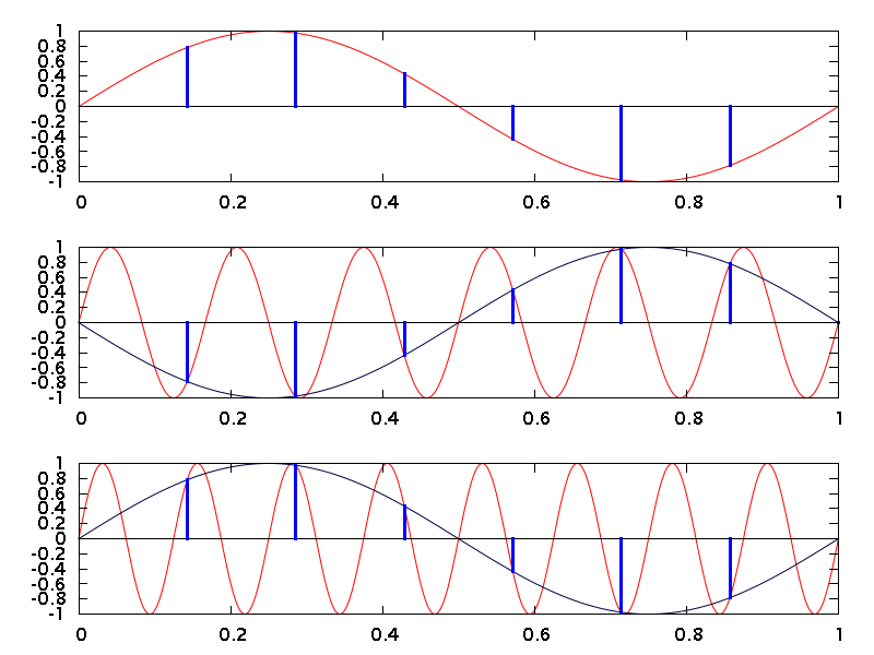
One phenomenon that happens with any analog-to-digital conversion is known as aliasing.  A-to-D is inherently a sampling process, in which an analog signal that is continuous in time is converted to a digital signal that exists in discrete chunks, or samples.  The rate at which those samples are taken is known as the sampling rate.  The figure below shows three analog sine waves, in red, being sampled at the times marked with the blue vertical lines.  The top sine wave has a frequency of 1 Hz, and it is being sampled at 7 Hz.  (The seventh sample is not obvious, because it is zero and the left- hand or the right-hand edge of the graph.  Which edge you choose is unimportant.)

A frequency above the sampling rate results in aliasing to a lower frequency

The second and third plots in the figure show aliasing in action.  When any signal with a frequency above one-half the sampling rate is sampled, the signal is <i>aliased</i> down to a frequency between 0 Hz and one-half the sampling rate.  The second line shows a 6 Hz sine wave in red, which is being sampled at 7 samples per second (sps).  The blue lines show where the samples fall.  Because 6 Hz is above 3.5 sps (one half of 7 sps), the sine wave will be aliased.  As you can see, the blue samples are identical to those you see in the top trace, except that they have the opposite polarity.  The dark blue trace connects them and shows that a 6 Hz sine wave is indistinguishable from a 1 Hz sine wave when both are sampled at 7 sps.  That is aliasing in action.

The same process happens for any input frequency above one-half the sampling rate.  The third plot in the figure, for example, shows an 8 Hz sine wave.  Again, it is sampled at 7 Hz.  This time the samples are identical to those in the top line.  The sampled waveform (in dark blue once again) is indistinguishable from the sampled version of our original 1 Hz sine wave.

Aliasing is so important that one-half the sampling rate has become known as the “Nyquist frequency” for a system.  You may see people refer to signals as being “above Nyquist” or “below Nyquist”.  Aliasing happens in a repeated pattern as the frequency rises, and each repetiion of that pattern is called a “Nyquist zone”.  All of this is in memory of Harry Nyquist (1889-1976), who with Claude Shannon discovered much of the mathematics behind sampling.

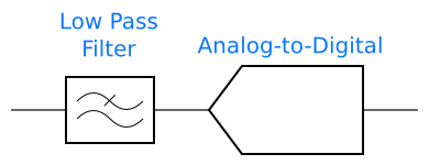
Because of aliasing, analog-to-digital converters are usually preceded by an anti-aliasing filter.  This filter removes the frequency content outside of the desired Nyquist zone, so that noise and interfering signals do not alias into the passband of the ADC.  Most often, a low-pass filter is used, so that the selected Nyquist zone runs from DC (0 Hz) to 1/2 the sampling frequency.  There are some exotic RF applications in which a bandpass filter selects frequencies in a higher Nyquist zone, which the ADC then aliases down, but these are uncommon.

An anti-aliasing filter before an ADC input.

How Oversampling Makes Anti-Aliasing Easier

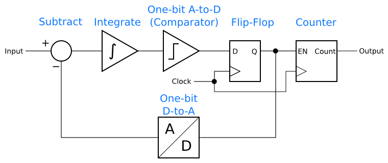
In order to get good accuracy, delta-sigma converters need to run at a much higher frequency than the input signal.  The first part of this series introduced an idea for an ADC built from a delta-sigma modulator followed by a digital counter:

Conceptual delta-sigma analog-to-digital converter

For this to work, the delta-sigma modulator has to <i>oversample</i>.  In order to have the counter reflect the input signal accurately, there have to be many 1 and 0 bits in the modulator’s output for the counter to count.  In other words, each sample from the counter’s output has to reflect many samples in the modulator.  This is called oversampling.

The nice thing about oversampling is that the Nyquist frequency goes up with the sample rate, even when oversampling!  The classic example of this happens in CD audio systems.  CDs carry audio signals of up to 20 kHz, with a 44.1 ksps sample rate and a Nyquist frequency of 22.05 kHz.  Furthermore, CD audio has a dynamic range of about 97 dB.  In order to avoid aliasing signals back into the 0 Hz – 20 kHz audio band, the antialiasing filter at the input of a CD audio ADC needs to have a rolloff frequency (-3 dB) at 20 kHz, and should be down to -97 dB by 24.1 kHz.  This is an impractical filter to design and build.

However, if an oversampled delta-sigma ADC is used, then the Nyquist frequency goes up to one-half the oversampled sample rate.  A typical choice might be 64x oversampling, in which case the ADC will sample at 2.8224 MHz.  Then the Nyquist frequency is 1.4112 MHz.  The anti-aliasing filter still needs to have its -3 dB rolloff at 20 kHz, but it does not need to be -97 dB down until 2.82 MHz.  That is a much easier filter to design.  In fact, a 3-pole filter, easily and cheaply implemented with an op amp, is sufficient.

Moving Anti-Aliasing to the Digital Domain

To go from 2.8 Msps to 44.1 ksps requires another round of sampling, this time in the digital domain.  Remember the counter?  The process of reading its count, then resetting it for another round of counting, is a form of sampling, and aliasing can result.  The figure below shows an example.  In this case, an 8 Hz sine wave is being sampled at 70 sps by an oversampling ADC.  Then, that digital signal is being downsampled, by taking every tenth sample, to 7 sps.  The result is that the 8 Hz input is aliased to 1 Hz, just as if it was sampled at 7 sps in the first place.

Aliasing can result from downsampling a digital signal.

Just as in the analog domain, there are times when the aliasing resulting from downsampling can be useful, but often it is not.  To prevent it, we need a low-pass filter, but this time the filter can be digital.  In the CD-audio example, the filter needs to have the same rolloff characteristics as the challenging analog filter (-3 dB at 20 kHz, and -97 dB at 24.1 kHz).  Doing that in a digital filter, though, is much easier than in analog.  Digital arithmetic can produce a filter of arbitrarily good performance, without the precision components or careful tuning adjustments that might be required in analog.  All it takes is throwing enough logic gates at the problem, and thanks to Moore’s Law, logic gates are cheap.

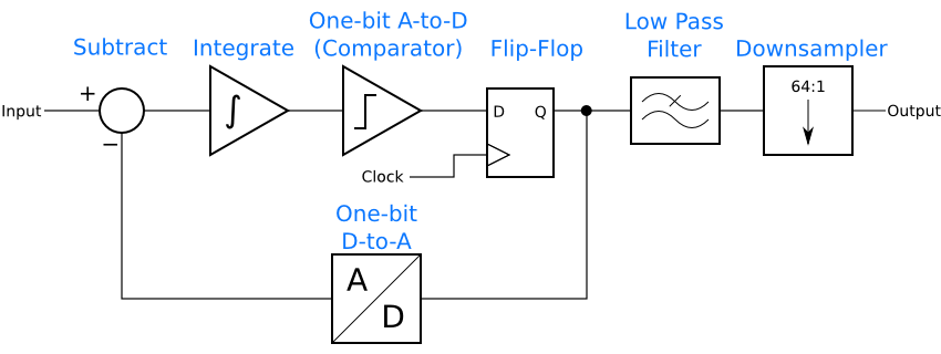
Since low-pass filters have an averaging effect, the filter will turn the bitstream of 1’s and 0’s into a series of multi-bit samples.  The counter becomes unnecessary.  Instead, it is enough to keep one sample from the low-pass filter’s output every so often, discarding the rest.  The ADC now looks like this.  (A simple anti-aliasing filter before the input is needed, but not shown.)

A delta-sigma ADC with a low pass filter and downsampler

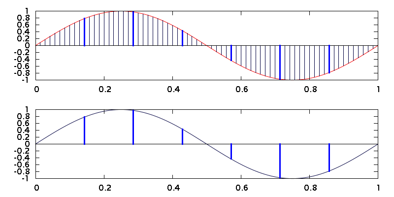
The figure below shows the principle.  A 1 Hz sine wave is oversampled at 70 Hz in the top graph, then 9 out of every 10 samples are discarded, leaving only the highlighted ones.  Those samples are plotted in the bottom graph.  The result is identical to the sine wave samples in the first graph at the top of this article.

Downsampling an oversampled signal is equivalent to sampling in the first place.

Technology similar to this, with some additional improvements to reduce the amount of math needed, makes it possible to put CD-quality ADCs in every desktop and laptop computer.  Instead of an expensive analog filter, cheap digital gates on an IC provide most of the filtering, reducing the cost of the ADC to only a dollar or two.

Wrapping Up

In this article, we have come full circle to find out how delta-sigma techniques can make analog design easier.  I’ve shown how aliasing happens and explained the need for anti-aliasing filters.  Then we looked at the oversampling inherent to delta-sigma modulators, and how that permits a simpler analog antialiasing filter, at long as a digital low-pass filter is included after the modulator.  This is just one of the reasons why delta-sigma principles are very cool.  Coming up in this series: Simulating a delta-sigma modulator and an introduction to noise shaping.

Reference

Bourdopoulos, George I., Aristodemos Pnevmatikakis, Vassilis Anastassopoulos, and Theodore Deliyannis.  Delta-Sigma Modulators: Modeling, Design and Applications. London: Imperial College Press, 2003

How Delta Sigma Works, part 1: Introducing the Delta Sigma Modulator

Today I’d like to turn to the fascinating topic of delta-sigma techniques. Delta-sigma is best known for its use in analog-to-digital and digital-to-analog converters, but it also has a potent role in digital signal processing and even in analog applications. By its nature, delta-sigma can reduce the amount of analog circuitry needed in a radio or other electronics, and what is left is often simpler and cheaper than what would otherwise be required.

Beyond that, delta-sigma techniques are nifty! The core concept is counter-intuitive at first glance, yet it offers all kinds of powerful applications.

This post is part of a series on delta-sigma techniques: analog-to-digital and digital-to-analog converters, modulators, and more. A complete list of posts in the series are in the How Delta-Sigma Works tutorial page.

Today I’d like to turn to the fascinating topic of delta-sigma techniques. Delta-sigma is best known for its use in analog-to-digital and digital-to-analog converters, but it also has a potent role in digital signal processing and even in analog applications. By its nature, delta-sigma can reduce the amount of analog circuitry needed in a radio or other electronics, and what is left is often simpler and cheaper than what would otherwise be required.

Beyond that, delta-sigma techniques are nifty! The core concept is counter-intuitive at first glance, yet it offers all kinds of powerful applications. Working at understanding delta-sigma techniques gives deep insights to many other areas of signal processing.

This is the first of a multi-part series on delta-sigma, which is too broad and deep a topic to cover in a single post. There will be some math, balanced with an intuitive approach to the circuits. I will also delve into the the practical, building delta-sigma data converters and sharing the schematics and results. I will be learning about delta-sigma along with you, so stay tuned for more in future posts.

The place to begin is with a first order delta-sigma modulator, which is the simplest variety of delta-sigma circuit. A first-order modulator has a structure like this:

Abstract first-order delta-sigma modulator

Continue reading “How Delta Sigma Works, part 1: Introducing the Delta Sigma Modulator”

The Plan

I’ve been thinking for some time about a DSP-based ham radio. After
considering and discarding more grandiose schemes, I was inspired by my
Norcal 40A. It and the original Norcal 40 are fairly simple and highly
reproducible (thousands were built). However, performance was not
sacrificed in the name of simplicity. Instead, the rig was carefully
designed to make the most of its NE602 mixers and crystal filter.

Why not try for the same goals in a DSP-based rig? In theory, one should
be able to subsume all of the IF and most of the RF and baseband into….

I’ve been thinking for some time about a DSP-based ham radio.  After
considering and discarding more grandiose schemes, I was inspired by my
Norcal 40A.  It and the original Norcal 40 are fairly simple and highly
reproducible (thousands were built).  However, performance was not
sacrificed in the name of simplicity.  Instead, the rig was carefully
designed to make the most of its NE602 mixers and crystal filter.

Why not try for the same goals in a DSP-based rig?  In theory, one should
be able to subsume all of the IF and most of the RF and baseband into the
DSP, leaving little but filtering components and a few amplifiers outboard.
The result would have a small number of components and would be fairly easy
to build.

I set a goal to build a self-contained radio, not a PC-based software defined radio.  It will be narrow band for simplicity.  As much functionality as practical will be done digitally.  Finally, the design should be reproducible by others.  That, in turn, means that it should be documented, it should use a low-cost DSP toolchain, and it should be insensitive to component variation.

Finally, I have an interest in delta-sigma techniques and multirate DSP, and the radio will be an excellent platform to explore and experiment with those technologies.

Continue reading “The Plan”