AK5388 ADC breakout board update

For the last month or two, a breakout board for the AKM Semiconductor AK5388 analog-to-digital converter has been my main project. Here’s an update on where it stands.

When I last posted about the board, I was waiting for parts to arrive so I could check their fit on a printout of the PCB. After the capacitor footprint error on the FPGA breakout board, I was feeling a bit cautious. The parts arrived and fit fine!  I checked out the ADC on its QFP footprint, and it was perfect. Then I tried the big capacitors on their EIA 3216 footprints, and those were fine, too.

Fixing the schematic

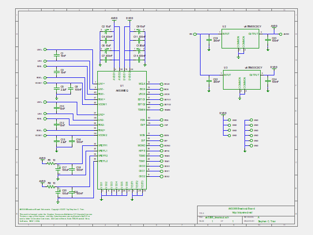
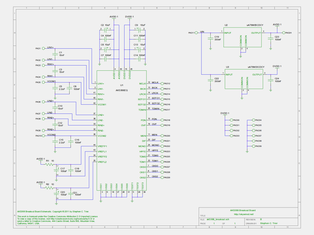
AK5388 breakout board schematic, revision B

I ran into some problems with the schematic when I did the PCB layout. One problem was that multiple pads named “GND” or “DVDD” were consolidated into one. A second problem was that the names I had assigned the pads were not visible in PCB, meaning I was in for a slow process of finding each one on the schematic in order to add the right label to the PCB’s silkscreen. I found a great solution, though.

The fix to both problems was to name the nets, not the pads. I restored all the pads to their boring PAD1, PAD2, … reference designators and named the schematic nets after the signals. Now, when I hovered the cursor over one of the pads in PCB, a little tooltip popped up and told me the net name connected to the pad, among other things. Labelling all of the pads took only a few minutes. I wish I had known about this trick when I did the A3PN250 FPGA board!

Secondly, using conventional reference designators to name the pads solved the problem with the DVDD and GND pads.

These changes resulted in the rev B schematic. A PNG version is above, and I’ll post the editable gschem version on the AK5388 breakout project page.

I have ordered the boards, and I will have more to say about that next week.

What do you think? Comments welcome!

Bus Pirate review

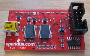
Sparkfun Bus Pirate, top viewThe Bus Pirate: It sounds kind of shady, and maybe it is, but it is also a handy little tool. A few weeks ago, I received a Sparkfun Bus Pirate as a birthday present. This little board is a USB-to-nearly-anything serial adapter that can speak SPI, I2C, async serial (UART), JTAG, and several other protocols. It’s designed as a quick tool for easy exploration of new hardware and, yes, as a hacking tool useful for reverse engineering undocumented boards and communications protocols. It has a few limitations that hold it back from being everything it could be, but the low price makes it a worthy addition to a professional’s or hobbyist’s engineering toolbox.

The Bus Pirate was designed by Ian Lesnet at Dangerous Prototypes, and he sells his original version via his partnership with Seeed Studio. Since it is an open source hardware design, others are free to make their own versions, which is what Sparkfun opted to do. It appears that Sparkfun did their own layout, but the major components are in roughly the same locations. Both versions are electrically equivalent and run the same firmware, and both versions cost about $30 (at this writing).

Bus Pirate Hardware and Accessories

On unpacking the box, my first surprise was the Bus Pirate’s small size. That’s not a drawback in practice, but it looks more delicate than I expected. The board has a row of LEDs along the top edge for status information, a USB mini-B connector on the left side, and a header for the serial interfaces on the right side. The header is shrouded, which is a nice touch, because it makes sure polarized cables only go in one way.

Polarization is great for cables, except that different versions of the Bus Pirate orient the header in opposite directions! The Sparkfun version has the polarization notch on the outside, while the Bus Pirate documentation says that some Seeed Studio versions have the polarization notch on the inside. Although this inversion means that pin “1” moves from one end to the other, the layout of the PC board has not changed, so the pin in the lower left corner remains chip select (CS), regardless of which way the header is installed.
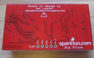
Bottom view of Sparkfun Bus PirateI am a little concerned about the durability of the board. One aspect is having small surface-mount components exposed, where they could get knocked off, taking their PCB pads with them. Another aspect is the choice of a USB mini-B connector. The mini-B has durability issues that has caused the USB Forum to deprecate it in favor of their other connector styles. A standard B connector would have been a better choice.
Another disappointment was the lack of PCB mounting holes, which are handy for screwing in standoffs to use as feet. holes would also make it easier to protect the board in an enclosure, such as a mint tin.  It appears that the latest Seeed Studio Bus Pirate boards (v3.5) have mounting holes.

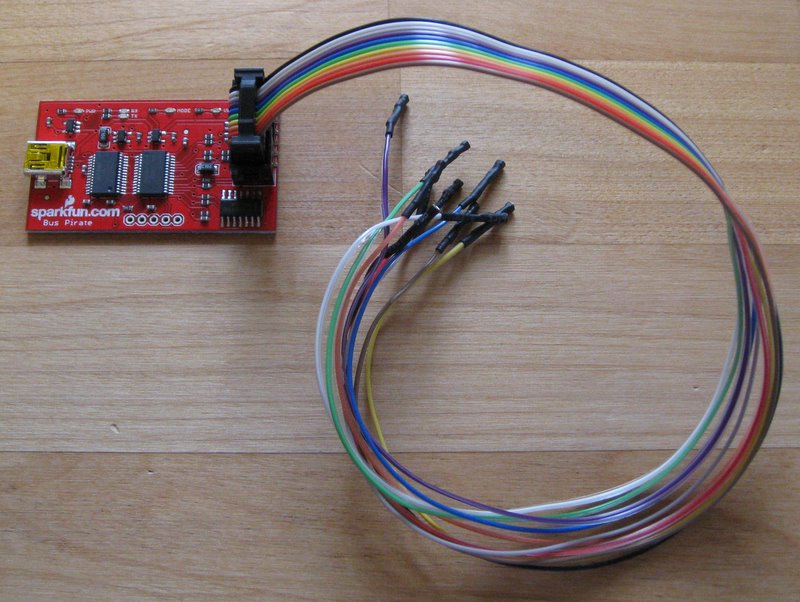
Sparkfun and Seeed both sell breakout cables for the board. These cables aren’t strictly necessary, and in fact you might find a fistful of single-pin jumpers more useful for many purposes. The header has a few pins that can be jumpered for special purposes, such as configuring a pullup voltage in open-drain/open-collector mode. The the breakout cable may make that more awkward in some circumstances. I found the breakout cable handy, though, and I would recommend it as an accessory. The Sparkfun cable has single-pin sockets on its loose leads.  Seeed sells a version with single-pin sockets and one with mini-grabbers.
SPI Sniffing

Although I wanted a Bus Pirate for my basement hacking, the day after I received it, I took it to work. I was debugging a tough problem for which it would be useful to be able to eavesdrop on SPI traffic between a microcontroller and a peripheral. The Bus Pirate’s SPI sniffer mode seemed perfect. (I did have the option of using an Agilent mixed-signal oscilloscope, but who wants to read hundreds of bytes, in binary, from a ‘scope screen when an easier option exists?)

In principle, SPI sniffing can be done from a terminal, but in practice, an SPIsniffer utility that uses the Bus Pirate in binary mode is recommended. I downloaded the SPIsniffer and had a tough time interpreting the output. It appears that the latest version was released with debugging code that causes duplicated bytes in the output. I removed the debugging code, recompiled, and had somewhat better success.
The SPI sniffer formats its output as “[0xba(0x00) 0x5e(0x00) 0x00(0x1e)]”. The square brackets show when chip select is active, and the bytes are shown as the MOSI value followed by the MISO value in parentheses. This format is basic, but easy to read. Getting the chip select brackets in the right place is critical to interpreting SPI traffic. Many chips use the first byte after chip select as a command or an address, and the following bytes as data. Without having chip select in the right place, it can be impossible to decipher the data stream.

Unfortunately, in my application, the chip select indications were all over. When watching an initialization sequence, which should have shown chip select low for each of a series of two-byte packets, and high in-between, the Bus Pirate showed many one-byte packets and a few with up to 10 bytes. I looked for ground loop problems and other issues that might throw it off, without success. An oscilloscope showed the two-byte packets, as expected. As best I can figure, the Bus Pirate was simply unable to keep up with the data stream and got its chip select reads out of sync with its serial data reads. The Bus Pirate did not drop any data bytes, but without accurate chip select information, it was as useless as if it had.

Would The Correct Logic Level Please Stand Up?

My SPI sniffing also brought to my attention the Bus Pirate’s less than ideal logic level selection. The Bus Pirate is billed as working with logic levels “at any voltage“, and “above and below the Bus Pirate’s 3.3V supply“. I thought this meant it incorporated a level shifter that could input and output all of the major logic levels used today, from 1.5V on up. Unfortunately, the truth is that the Bus Pirate runs at 3.3V with 5V-tolerant inputs. It does have the ability to use open-drain outputs with a strappable pull-up voltage, which could be anything from 0 V to 5V, but that does not change the input thresholds, which remain at standard 3.3V CMOS levels. Unfortunately, that means that logic running at 2.5V and below is not guaranteed to be read correctly by the Bus Pirate. Logic with a 1.5V supply simply won’t work.  (In fairness, there are other pages on the Dangerous Prototypes web site that correctly describe the Bus Pirate as supporting 3.3V and 5V I/O.)

This problem could be solved by incorporating a proper level shifter into the board or, with some constraints, by replacing the 3.3V regulator with a lower voltage version. The hobbyist market for which the device was designed rarely uses I/O voltages below 3.3V, so many typical users will not notice this limitation, at least for the next few years. However, the problem makes it harder to use the Bus Pirate as a reverse-engineering tool and for developing low-voltage designs.

A USB UART

The Bus Pirate includes a UART mode that lets it communicate with asynchronous serial, just like RS-232, but at logic levels. Conveniently, I’m currently working on a project that uses asynchronous serial at logic levels, but at an unusual baud rate. This was a great chance to try out the Bus Pirate.

In addition to all of the standard baud rates, UART mode accepts direct programming of the PIC’s baud rate generator. It was a simple matter to compute the right value for my project.

Unfortunately, though I was able to generate serial at the right baud rate and verify it on a ‘scope, I wasn’t able to get the Bus Pirate to work on receive. I had some noise problems with the system, and that coupled with the I/O voltage mismatch meant the receiver picked up garbage characters. I was in the midst of bringing up a custom USB-to-async converter to fill the same role, so I didn’t have much incentive to spend more time getting the Bus Pirate to work. I have since taken the time to eliminate the noise, so maybe the Bus Pirate would work now despite the logic-level mismatch. In any event, the problems on receive were my fault, not the Pirate’s.

Documentation

The Bus Pirate “manual” is a wiki. The strong point of using a wiki is that it is easy for the developers to update. It has some drawbacks, too. Like much hypertext documentation, there is no obvious way to read it linearly like a textbook, and it can be hard to be sure you have found all of the material relevant to a particular topic. Maybe I’m showing my age, but I would have liked to be able to download and archive a PDF, or perhaps even print and bind a manual with complete instructions for the Bus Pirate.

The documentation is concise to the point of terseness at times, but I was able to find all of the information I needed. The diagrams, in particular, are well done and clearly show exactly what needs to be conveyed.

Terminal Software

For some reason, the Bus Pirate did not work well with Windows’ Hyperterminal. From the wiki and forums, it seems this is not unusual. Following the manual’s recommendation, I switched to Tera Term and did not have any further problems.

More Cool Features

So far, I have only sampled the Bus Pirate’s capabilities. Among its cool features are a bitbang I/O mode that let the PC command each pin individually. Even in the SPI and other modes, it has an auxilary output pin that might be useful for a reset, address, or secondary chip select.

The Bus Pirate has two power supply outputs, one each at 5 V and 3.3 V, on its connector. Commands from the PC switch the supplies on and off, and there is enough current available to power small circuits. Some applications require little more than a Bus Pirate, a breadboard, and the target chip.

Analog signals can be read with the Bus Pirate’s ADC input pin. Together with the power supplies, this means that the Bus Pirate can directly connect to some analog sensors as well as the more obvious one-wire, I2C, and SPI devices.

It can even speak JTAG for debugging or programming, albeit slowly. It was not designed for JTAG and has to emulate the protocol in software.

The Bus Pirate also has a logic analyzer mode. SUMP and other software compatible with the Open Bench Logic Sniffer can interface to the Bus Pirate to read a few logic channels, slowly. It’s really just a toy in this mode, but I would have loved something like it when I was a kid experimenting with 4000-series CMOS.

Conclusions

I’m happy with my Bus Pirate. It is described as being a hacker’s multitool, and I have to agree. I love my Leatherman, too! I’m going to need longer to fully understand the Bus Pirate than to grok a Leatherman, but I’m looking forward to finding new ways to use it. Especially considering the low price, the Bus Pirate is a worthy addition to any basement tinkerer’s toolkit.

Is the Bus Pirate ready for professional use? The answer is “maybe”. If you work on 3.3V or 5V systems, buy one. It’s worth having in your toolbox, and the $30 price is practically free compared to engineering hours. I’m not quite ready to order some for my bench at work, though, because everything I do is at lower voltages. The low cost may yet pull me in, though. Particularly when evaluating new parts, the Bus Pirate would be a faster and easier solution than either a microcontroller or a National Instruments DAQ.

Links:
PCB routing techniques for ADCs

PCB layout is fun, especially when you are trying to eke the best performance out of a component.  Last week, I finished the PCB layout for the AK5388 analog-to-digital converter (ADC) I chose for my digital ham radio transceiver project. Let’s take a closer look at some of the design details…

My top priority was to keep digital lines away from sensitive analog signals. The quickly-switching edges of digital signals carry lots of high-frequency components, which readily couple into any neighboring line. It’s best to keep this high-frequency crud away from quiet analog signals. It’s not great to let it couple instead into other digital lines, but digital inputs are pretty tolerant to it and rarely have problems.

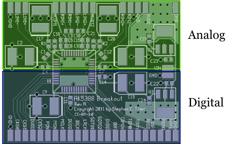
AK5388 board with an overlay showing how the analog and digital sections are separate.

The AK5388 pinout helps a lot with this separation requirement. As is done in many ADCs, all of the digital pins are on one side of the chip, and all of the analog pins on the other. When laying out a mixed-signal board (that is, one that has  both analog and digital elements), I like to draw a line across the board before I even start to place the parts, with all analog components going on one side and all digital on the other. As the placement and routing progress, that line will move and may even change into a zig-zag, but the idea remains: Keep the analog stuff on one side and the digital on the other.

On the AK5388 breakout board, the analog-digital border remains a straight line. Everything in the top half of the board is analog, and everything in the bottom half is digital.

Another reason to have a clean split is the return currents and their IR drop. Remember that current flows in a loop. When any of those digital lines changes state, it charges a small capacitance at the other end, and the current used to do that charging flows back through the ground plane. At high frequencies, that return current is largely confined beneath the digital line that caused it. On top of that, the return current causes a voltage gradient underneath it, thanks to Ohm’s law and the resistance of ground. (V = IR)  This voltage gradient can act as an additive noise source on analog signals that are routed near it. The careful split in this board’s design will help keep the digital return currents from affecting the analog signals.

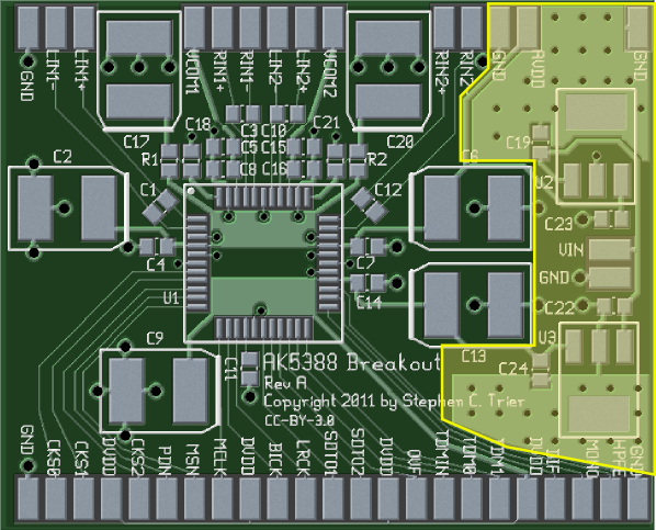
Another feature of the board is that it has local analog and digital power supplies for the ADC. The power supplies are located in their own area, again to try to limit noise caused by the return currents. In the picture below, the power supplies are highlighted in yellow.

The AK5388 breakout board with the power supply location highlighted.

The voltage regulators used here (uA78M33CDCY and uA78M05CDCY) are in SOT-233 packages, which have a large lead on one side to help with heatsinking.  The board is laid out with some extra copper area to act as a heat spreader for each SOT-223, along with a bunch of vias tying the top-side copper to the ground plane. These vias have a thermal role, not primarily an electrical one, as they help transfer heat from the top-side heat spreader down to the ground plane to further spread it out.

Although there are ways to estimate the thermal performance of a heat-spreader design like this, I didn’t do them. Frankly, I don’t have any idea whether this board’s thermal provisions are adequate. Even at the bargain price of $5/square inch to have this PCB fabbed, adding copper just for thermal management gets expensive. If the heat-spreading area turns out to be insufficient, I’ll find a way to attach a heatsink to the top side of the regulators, solder a piece of brass to their large lead, or something along those lines to remove the heat more efficiently.

Finally, take a look at the decoupling capacitors. C4, C7, C11, and C14 are 100 nF capacitors, each on one power-supply input to the ADC. They are positioned as close to the ADC as I could manage. One could argue that their positioning is not quite perfect because there is a relatively long path from their grounded side to the closest ADC ground pin. It goes through two vias and the ground plane. I have never looked into whether this makes a significant difference. If you know, leave a note in the comments and tell me!

In any case, the 100 nF capacitors are multi-layer ceramic capacitors (MLCC), which have a low equivalent series resistance (ESR) and inductance (ESL). Those characteristics make them ideal for decoupling high-frequency noise on the power supply lines.

Next, C2, C9, C22, and C23 are big 10 μF decoupling capacitors. These are positioned a little farther away. They are aluminum electrolytic capacitors, which have a higher ESR and ESL than ceramic caps. (10 μF ceramic capacitors are expensive!) These capacitors are better for removing low frequencies, including the audio range, from the power supplies. For that reason, I did not see much harm in putting them a little farther from the ADC, with the extra inductance and resistance that implies. Besides, these things are BIG! If they were any closer to the ADC, routing the signal lines in and out would get pretty challenging.

One trick for getting the decoupling capacitors closer is to put them on the back side of the board. The distance through a via would be much shorter than the distance needed here. I wanted a single-sided design here, so that wasn’t an option, but it’s something to keep in mind.

I won’t claim that I know everything about designing for a high-performance ADC. In fact, it’s possible that someone more experienced is planting their face in their palm right now, saying, “I can’t believe he did that!”  (If that’s you, by the way, drop me a note to let me know what the problem is, would you?)  That said, what I did here is based on app notes and other materials from a number of semiconductor companies, including Analog Devices and National Semiconductor, and I think it’s pretty sound.

I ordered the parts for this board today. It doesn’t take long for UPS to get things to Ohio from Digi-Key’s home in northernmost Minnesota, but it’s always a long wait when I’m itching to try something out.

I’ll catch you next week with more on electronics, DSP, and ham radio.

PCB layout for the AK5388 ADC breakout board

I had some time to myself this weekend and was able to get the AK5388 breakout board routed. The board carries an AKM AK5388 audio DAC, which has 24-bit output and up to a 123 dB signal-to-noise ratio. My plan is to build up this board, evaluate it to verify that it works as I expect, then use it as the ADC stage in a DSP-based ham radio receiver.

Moving the schematic from gschem to PCB was really easy. This was my first time using PCB’s “Import schematics” command. It was a breeze, especially compared to the old way of doing it, the gsch2pcb command. That command worked well enough, but I could never get it done without checking the documentation or a howto online. “Import Schematics” required no such thing. Bravo to the PCB developers!

As with the FPGA board, I laid out the board with a solid groundplane on the back and all components and traces on the front. That way, it can be placed on a piece of copperclad board, for skywired construction, without risk of shorts to ground. It’s also good for noise performance.

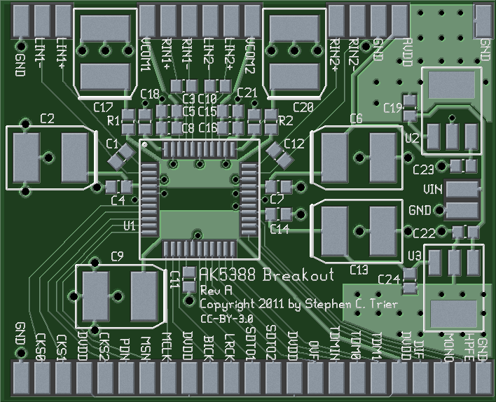
Photorealistic view of AK5388 breakout board, top side

The square chip in the middle (QFP, U1) is the AK5388. On the right edge are a 7833 and a 7805 voltage regulator, for the digital and analog power supplies, respectively. The board includes some heatsink area around the regulators (U2 and U3), with thermal vias to stitch the heatsink to the groundplane on the back. The rest of the components are decoupling capacitors, lots of decoupling capacitors, plus two resistors that also help control noise. A 24-bit ADC needs quiet power supplies!

As you might expect, the bottom side is kind of boring:

Photorealistic image of the bottom side of the AK5388 breakout board

That’s the ADC board so far. Although I have Gerber files now and could go order the boards, I’m going to order the parts first this time and test-fit them on a printout of the layout.

gedasymbols.org is a great part of using gEDA

I’ve joined up as a contributor to  gedasymbols.org. This great resource, run by DJ Delorie, hosts schematic symbols for gschem and footprints for gEDA’s layout software, PCB. A search engine helps locate symbols and footprints, and gedasymbols includes links to other libraries off-site, such as Dan Luciani’s extensive footprint library. Gedasymbols.org has been hugely useful every time I do a design in gschem or PCB, and I’m happy to have something I can contribute back.

Gedasymbols has the symbols and footprints for the A3PN250 FPGA and AK5388 audio ADC breakout boards, plus symbols from an MSP430 project that I haven’t posted here yet.

As for other hacking recently, I’ve done parts placement for the AK5388 board but haven’t started routing it. I also need to make a better feedthrough panel for my antenna. I’ll have more to say about those two projects in a future post.

Comments welcome!

AK5388 audio ADC breakout board design

A few weeks ago, I picked the AKM Semiconductor AK5388 as the analog-to-digital converter for my receiver design. This high-performance audio DAC has a 24-bit output with up to 123 dB signal-to-noise ratio (A-weighted).  I hope that the narrower bandwidths of a communications receiver will beat that. The idea is to do the automatic gain control (AGC) in digital, so that the receiver will not need an analog AGC loop. I hope that a preamp or attenuator at the front end will be enough to make up for the limited dynamic range of the AGC.

Now, I am aware that getting performance like that requires great care in the details of the design and layout, but if this wasn’t a challenge, it wouldn’t be nearly as much fun!  The AK5388 datasheet does give me some concern, because it does not make much mention of the techniques needed for a high-performance DAC. Admittedly, datasheets from Japanese manufacturers are often thinner on details than those from the leading US suppliers, and this one is much more complete than some. On the other hand, it may be that the datasheet is glossing over any coddling this chip will need.

There is one way to find out, and that is to start breadboarding. This is a surface-mount part, so I have designed a breakout board very much like the board I built for the Actel Microsemi A3PN250 FPGA. The schematic is below.

AK5388 ADC Breakout Board schematic

The schematic largely follows the “System Design” section of the datasheet and the example of the AKD5388-A evaluation kit (PDF). It’s not strictly a breakout because I included on-board analog and digital power supplies. An ADC like this needs quiet, local power, so I picked some reasonably quiet supplies and put them on-board. I chose 7800-family regulators from TI because they have reasonable noise specifications. I almost went with other choices that were explicitly designed for low noise, but they were quite a bit more expensive for not much less noise. The AKD5388-A kit uses an uA78M05 and claims to be able to obtain the full dynamic range of this ADC, so there is little reason to spend more at this point.

I’m using the analog power supply as the voltage reference. I considered a dedicated reference, which would be more expensive but perhaps lower noise. Here, too, I followed the lead of the evaluation kit.

The PCB layout should be straightforward. I like to build by skywiring components over a groundplane, so this breakout board will be designed to sit directly on a groundplane, with all components and connections on the top side. All external wiring points will be pads on the PCB, ready for soldering, just as with the A3PN250 FPGA board.

I’m excited about trying out this part. What do you think? Comments welcome!