FPGA Breakout Board Layout

Here at last is the printed circuit board layout for the FPGA breakout board. I’m planning a series of projects involving FPGA-based DSP for ham radio, and in order to build them, I need an FPGA and a PCB on which to mount it….

The goals for this layout constrained it to be a nearly single-sided layout, …

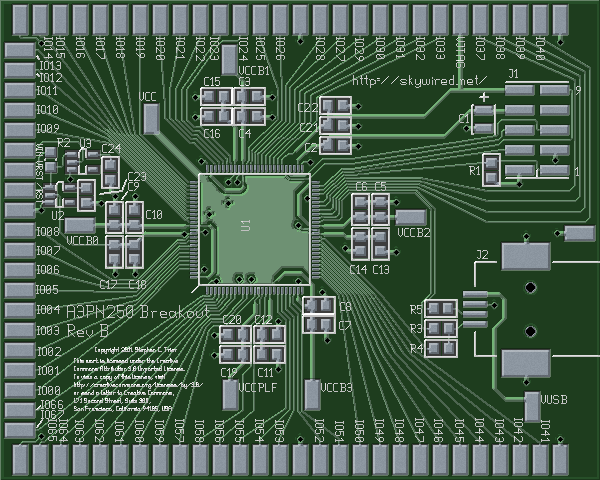
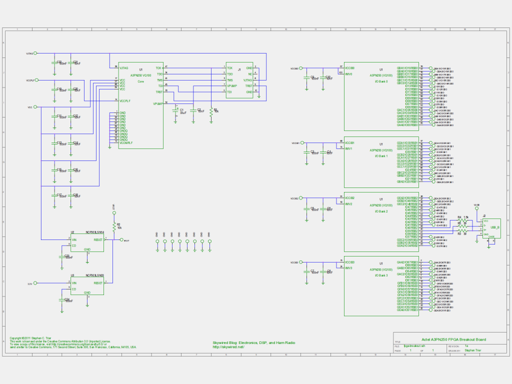
Here at last is the printed circuit board layout for the FPGA breakout board. I’m planning a series of projects involving FPGA-based DSP for ham radio, and in order to build them, I need an FPGA and a PCB on which to mount it. In the last installment of the project, I presented the schematic for the breakout board.

The goals for this layout constrained it to be a nearly single-sided layout, with a ground plane on the back. That way, the board could be mounted directly on a piece of copperclad with no short circuits to ground. My budget limited me to a double-sided board, so all signal and power traces had to go on the top side.

That said, here is the layout, top and bottom.

FPGA breakout PCB, top side

Continue reading “FPGA Breakout Board Layout”

FPGA Breakout Design Decisions

To get to my goal of a DSP-based ham radio using an FPGA as the DSP, I first need a way to prototype with an FPGA. Available FPGAs all use modern, small packages such as QFNs, QFPs, and BGAs. I can’t imagine soldering wires directly to a hundred tiny pins, so “dead-bug” construction, with the chip upside-down on a piece of copperclad board, is out. I need a breakout PCB that holds the chip and brings out its pins to something more reasonable to work with.

To get to my goal of a DSP-based ham radio using an FPGA as the DSP, I first need a way to prototype with an FPGA.  Available FPGAs all use modern, small packages such as QFNs, QFPs, and BGAs.  I can’t imagine soldering wires directly to a hundred tiny pins, so “dead-bug” construction, with the chip upside-down on a piece of copperclad board, is out.  I need a breakout PCB that holds the chip and brings out its pins to something more reasonable to work with.

Continue reading “FPGA Breakout Design Decisions”

The Plan

I’ve been thinking for some time about a DSP-based ham radio. After
considering and discarding more grandiose schemes, I was inspired by my
Norcal 40A. It and the original Norcal 40 are fairly simple and highly
reproducible (thousands were built). However, performance was not
sacrificed in the name of simplicity. Instead, the rig was carefully
designed to make the most of its NE602 mixers and crystal filter.

Why not try for the same goals in a DSP-based rig? In theory, one should
be able to subsume all of the IF and most of the RF and baseband into….

I’ve been thinking for some time about a DSP-based ham radio.  After
considering and discarding more grandiose schemes, I was inspired by my
Norcal 40A.  It and the original Norcal 40 are fairly simple and highly
reproducible (thousands were built).  However, performance was not
sacrificed in the name of simplicity.  Instead, the rig was carefully
designed to make the most of its NE602 mixers and crystal filter.

Why not try for the same goals in a DSP-based rig?  In theory, one should
be able to subsume all of the IF and most of the RF and baseband into the
DSP, leaving little but filtering components and a few amplifiers outboard.
The result would have a small number of components and would be fairly easy
to build.

I set a goal to build a self-contained radio, not a PC-based software defined radio.  It will be narrow band for simplicity.  As much functionality as practical will be done digitally.  Finally, the design should be reproducible by others.  That, in turn, means that it should be documented, it should use a low-cost DSP toolchain, and it should be insensitive to component variation.

Finally, I have an interest in delta-sigma techniques and multirate DSP, and the radio will be an excellent platform to explore and experiment with those technologies.

Continue reading “The Plan”