R2 receiver update: Time for new electrolytic capacitors

Crunch time at work has been limiting my basement tinkering, but I recently found time to work on my R2 receiver a bit more. It is pulling excessive bias current, which had me scratching my head. The audio power amplifier bias is supposed to be adjusted so that the whole board pulls 100 mA, but it’s taking 120 mA even with the bias pot set to its minimum. After double-checking all of the component values and verifying all of the bias voltages on the board, I was left scratching my head. Then I remembered the age of the kit. Even while building it, I had doubts about the electrolytic capacitors…

This R2 kit includes 15 Panasonic Z-series electrolytic capacitors. Aluminum electrolytic caps are good at one thing: Lots of capacitance at a low cost. In nearly every regard, they have inferior performance, with high equivalent series resistance (ESR), inductance (ESL), and, yes, a short lifetime. I’m not sure exactly how to translate the lifetime specifications for electrolytics to room temperature storage, but the rule of thumb tends to be that they can tolerate 5 years on the shelf, after which they require a “reforming” procedure. Reforming them at that point can get them to last another 5 years or so. After that, figure that they are shot. Old electrolytic capacitors can have excessive leakage current. In extreme cases, this current is enough to heat them up excessively and they go bang! The capacitors on this board are old enough to vote. Maybe one or more of them are to blame for the extra milliamps.

I had a little trouble finding the perfect capacitors, but then I was looking for performance at least as good as the original. This was perhaps foolish, because I couldn’t find data on the Z-series caps. Panasonic discontinued them in 2000. In lieu of further information, I arbitrarily went for high-quality models from a favorite manufacturer. In some cases, these were nearly double the price of the cheapest options, a breathtaking 23 cents versus 12 cents, quantity one. Seriously, replacements for all of the caps cost all of $2.85, including a few spares for good measure.

My one mistake so far is to forget about the T2 transmitter. If the R2’s capacitors are bad, the T2’s surely are as well. Maybe the spares I bought will end up there.

Troubleshooting is half the fun of this stuff. Who needs sudoku when you can puzzle out a misbehaving circuit?
Building a KK7B R2 phasing receiver

Hi, I’m back! It was a rough week, with a death in the family. As it ended, I found some time for some “solder therapy”. There is something good for the soul in putting together electronics. I don’t know if it’s the scent of the rosin or the satisfaction of seeing a project come together. All I know is it’s good for me.

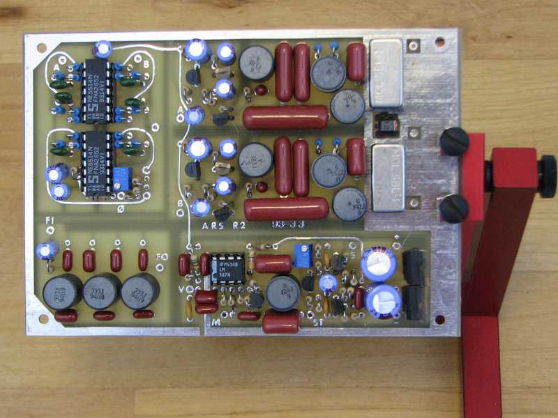
KK7B R2 receiver, top side

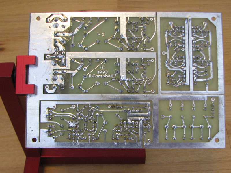
The target of my soldering was my KK7B R2 receiver kit. This is the companion to the T2 I wrote about a few weeks ago. To my surprise, the R2 was easier to put together despite the higher part count. The components are larger, forcing a less dense pin matrix, and the board is separated into sections: mixers and diplexers, audio phase shift, low-pass filter, and audio amplifier. Conveniently, the board uses jumper wires (not yet installed on mine) to connect the sections. The intent appears to have been to make it easier to extend the board by swapping in a different phase shift network or adding alternate filters for CW or contesting, but it will make the board easier to debug as well, since I can bring it up a section at a time.

Keep in mind that this is a vintage kit that is no longer available, but updated versions of the design are still produced by Kanga US.

The board surprised me with its heft. I work mostly with surface-mount digital boards where the fiberglass PCB is the heaviest component. This board, though, weighs 134 g (4.7 oz), which is a lot for 100 cm2 (16 in2). The shielded inductors are the culprits. Each black cylinder in the photo is the ferrite shield of an inductor. Each inductor is noticeably heavy for its size, and this board has 10 of them.

KK7B R2 receiver board, bottom side

Once I wash the flux off (it’s not as much fun as soldering), the next piece of the puzzle is to build or buy a VFO. Rick, KK7B, designed a companion VFO for these boards, but it is out of production at the moment. I’m thinking about one of the Si570 VFOs out there. This little chip offers a very low phase noise synthesizer with tuning in steps of a fraction of a Hertz. Having this on a single chip was a pipe dream when the R2 and T2 were designed.

After that, I’ll need to build a power amplifier to boost the T2’s milliwatts up to a reasonable level — at least a watt, maybe as much as 50 W. Finally, I will have to integrate all the pieces into a working rig. Professionally, I do a lot of microcontroller work, so it’s tempting to build a fancy digital control panel with circuitry to integrate every R2 and T2 option imaginable. Instead, I’m trying to keep myself to something simple: one band, SSB only, and a digital frequency readout as the only frill.

I still have to pick the initial band. I’m torn between 20m, my favorite for PSK31, and 40m, which I like for SSB. I’m after whatever DX I can land in either mode. What band would you recommend?

AK5388 audio ADC breakout board design

A few weeks ago, I picked the AKM Semiconductor AK5388 as the analog-to-digital converter for my receiver design. This high-performance audio DAC has a 24-bit output with up to 123 dB signal-to-noise ratio (A-weighted).  I hope that the narrower bandwidths of a communications receiver will beat that. The idea is to do the automatic gain control (AGC) in digital, so that the receiver will not need an analog AGC loop. I hope that a preamp or attenuator at the front end will be enough to make up for the limited dynamic range of the AGC.

Now, I am aware that getting performance like that requires great care in the details of the design and layout, but if this wasn’t a challenge, it wouldn’t be nearly as much fun!  The AK5388 datasheet does give me some concern, because it does not make much mention of the techniques needed for a high-performance DAC. Admittedly, datasheets from Japanese manufacturers are often thinner on details than those from the leading US suppliers, and this one is much more complete than some. On the other hand, it may be that the datasheet is glossing over any coddling this chip will need.

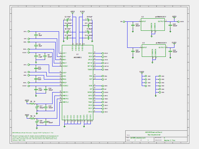
There is one way to find out, and that is to start breadboarding. This is a surface-mount part, so I have designed a breakout board very much like the board I built for the Actel Microsemi A3PN250 FPGA. The schematic is below.

AK5388 ADC Breakout Board schematic

The schematic largely follows the “System Design” section of the datasheet and the example of the AKD5388-A evaluation kit (PDF). It’s not strictly a breakout because I included on-board analog and digital power supplies. An ADC like this needs quiet, local power, so I picked some reasonably quiet supplies and put them on-board. I chose 7800-family regulators from TI because they have reasonable noise specifications. I almost went with other choices that were explicitly designed for low noise, but they were quite a bit more expensive for not much less noise. The AKD5388-A kit uses an uA78M05 and claims to be able to obtain the full dynamic range of this ADC, so there is little reason to spend more at this point.

I’m using the analog power supply as the voltage reference. I considered a dedicated reference, which would be more expensive but perhaps lower noise. Here, too, I followed the lead of the evaluation kit.

The PCB layout should be straightforward. I like to build by skywiring components over a groundplane, so this breakout board will be designed to sit directly on a groundplane, with all components and connections on the top side. All external wiring points will be pads on the PCB, ready for soldering, just as with the A3PN250 FPGA board.

I’m excited about trying out this part. What do you think? Comments welcome!

Choosing a high-performance audio ADC

As I discussed two weeks ago, it is time to refocus my efforts on the DSP-based ham radio project that started this blog. Let’s take a look at the architecture I had in mind originally:

Block diagram of a near-zero IF receiver with I and Q paths

This is a popular topology for radios that put their intermediate frequency at or near 0 Hz. It is also very similar to the most popular ham software-defined radio topology. In fact, those ham SDRs simply substitute a PC sound card for the ADC and the PC’s CPU for the FPGA. Here, though, I don’t want to bring a PC into the picture yet. Radios that require a PC don’t feel like “real radios” to me. I want to end up with a self-contained box, though I won’t mind if it optionally integrates with a PC.

For simplicity, I want to implement the receiver’s automatic gain control (AGC) functional digitally, after the ADCs. This means that with a well-designed front end, the ADC dynamic range will become the radio’s dynamic range.

With that in mind, I went looking for the best dynamic range audio ADC I could find, or at least the best one I could afford. I have identified seven manufacturers of 24-bit audio ADCs. Here is the best that they have:

Part SNR, A-weighted THD+N Package Price
TI PCM4222 123 dB -108 dB TQFP-48 $29.99 D*
TI PCM4220 123 dB -108 dB TQFP-48 $19.10 M
AKM AK5388 123 dB (Note 1) -110 dB LQFP-44 $10.93 D
AKM AK5394A 123 dB -110 dB SOP-28 $22.00 D
Cirrus CS5381 120 dB -110 dB SOIC-24, TSSOP-24 $32.22 D/M
Wolfson WM8786 111 dB -102 dB SSOP-20 $3.48 M
ADI AD1974 105 dB -96 dB LQFP-48 $10.03 D
NXP UDA1361 100 dB -88 dB SSOP-16 $1.37 M
Notes: 

Figures are typical values as shown in the manufacturer’s data sheet. All are for two channels active and 24-bit PCM output. Prices are quantity 1 from the cheaper of Digi-Key or Mouser.

1. The AK5388 is a four-channel ADC with 120 dB SNR. The 123 dB SNR requires the use of “mono mode”, which connects each stereo pair in parallel with a single input, effectively creating a two-channel ADC with 3 dB better SNR.

* Non-stock item, but a limited number of units are currently in stock.

The AK5388 looks like the price/performance winner, at $10.93 for 123 dB SNR and the best THD+N. One catch is figuring out the mono mode, which didn’t have crystal-clear documentation in the data sheet. On the other hand, even in four-channel mode it has 120 dB SNR, which still puts it at an excellent price/performance point.

Lurking in the SNR specification is A-weighting, which is a specification used for audio that isn’t much seen in the measurement world. The idea behind A-weighting is to reflect the human ear’s varying perception of noise at different frequencies by doing a weighted sum of the noise in the SNR measurement. Thus, frequencies where noise is more audible count worse than frequencies where it isn’t. A-weighting is not quite the right measurement for a near-zero IF ADC, first because a communications receiver’s bandwidth is quite a bit smaller than the 20 kHz used for the A-weighted measurement, and second because the communications signal being digitized is not necessarily at its final audible frequency yet.

I used A-weighting for the comparison because all of the ADCs were specified that way. Some of them also had an SNR in 20 kHz bandwidth specification, which does not weight the noise spectrum. For those ADCs, the 20 kHz SNR was 3 dB lower than the A-weighted SNR. , I decided to compare the A-weighted SNR to put the ADCs on equal ground, even though the 20 kHz bandwidth SNR is closer to what I would like to know for a communications receiver.

It’s worth mentioning that I looked at precision ADCs as well. I couldn’t find any 24-bit precision ADCs from Analog Devices or Linear Technologies that had a high-enough sample rate to be usable. In contrast, TI offers the single-channel ADS1281 and ADS1282, which offer a stunning 130 dB SNR (unweighted) at 250 samples per second. These might be reasonable for a Morse code receiver with a 100 Hz passband. When used for sideband, these ADCs would have to be operated in their 4000 SPS mode, at which their SNR drops to 118 dB. When one considers that filtering the output of the audio ADCs down to 100 Hz would provide an extra 6+ dB of SNR (because less bandwidth means less noise power), the ADS1281/1282 no longer has such an advantage. Worse, a pair of ADS1281 (two are needed because they are single-channel) will set you back $108 at Digi-Key.

In the end, I’ve found a combination of excellent performance and a good price. The AK5388 it is. The next step is to build or buy a board for it so I can start experimenting.

The FPGA level shifter: not entirely crazy!

Some months ago, I came across an Actel app note that advocated using FPGAs as level shifters. “What a crazy waste of computing power,” I thought to myself, “though I suppose they are just trying to sell the low-end ProASIC3 nano FPGAs.” With that, I set the thought aside.

Much later, I ran into a problem.

Some months ago, I came across an Actel app note that advocated using FPGAs as level shifters. “What a crazy waste of computing power,” I thought to myself, “though I suppose they are just trying to sell the low-end ProASIC3 nano FPGAs.”  With that, I set the thought aside.

Much later, I ran into a problem. I had a prototype board to design. It had to plug into an existing, quite complicated microprocessor evaluation kit, adding a data radio and a few other functions to the system. After poring over the schematic for hours, the software developer, who I’ll call S, and I still weren’t 100% sure which pins on the expansion bus were free for our use, though we had a long list of pins that definitely were not suitable. On top of that, I had a level-shifting problem. The evaluation kit ran at 1.8 V and 2.75 V, with signals at both levels on the bus, but the radio required 3.3 V logic levels. Continue reading “The FPGA level shifter: not entirely crazy!”

The Plan

I’ve been thinking for some time about a DSP-based ham radio. After
considering and discarding more grandiose schemes, I was inspired by my
Norcal 40A. It and the original Norcal 40 are fairly simple and highly
reproducible (thousands were built). However, performance was not
sacrificed in the name of simplicity. Instead, the rig was carefully
designed to make the most of its NE602 mixers and crystal filter.

Why not try for the same goals in a DSP-based rig? In theory, one should
be able to subsume all of the IF and most of the RF and baseband into….

I’ve been thinking for some time about a DSP-based ham radio.  After
considering and discarding more grandiose schemes, I was inspired by my
Norcal 40A.  It and the original Norcal 40 are fairly simple and highly
reproducible (thousands were built).  However, performance was not
sacrificed in the name of simplicity.  Instead, the rig was carefully
designed to make the most of its NE602 mixers and crystal filter.

Why not try for the same goals in a DSP-based rig?  In theory, one should
be able to subsume all of the IF and most of the RF and baseband into the
DSP, leaving little but filtering components and a few amplifiers outboard.
The result would have a small number of components and would be fairly easy
to build.

I set a goal to build a self-contained radio, not a PC-based software defined radio.  It will be narrow band for simplicity.  As much functionality as practical will be done digitally.  Finally, the design should be reproducible by others.  That, in turn, means that it should be documented, it should use a low-cost DSP toolchain, and it should be insensitive to component variation.

Finally, I have an interest in delta-sigma techniques and multirate DSP, and the radio will be an excellent platform to explore and experiment with those technologies.

Continue reading “The Plan”