Freescale’s SDR on a Chip

Freescale has introduced a very nifty part, the MC13260 SoC Radio, where SoC is “System on a Chip”.  Picture for a moment a complete transceiver on a chip, including an 100 MHz ARM processor, a programmable DSP modem, a frequency synthesizer, a transceiver, a USB interface, an audio CODEC (for the microphone and speaker), and miscellaneous support components, all on one chip.

The thing operates at RF frequencies from 60 to 960 MHz. It’s designed primarily for analog FM and certain digital modes, but with an external modulator it can support linear modes, presumably including SSB.  Output is only 5 dBm, so the advertised “few external components” had better include an amplifier!

Though the chip is aimed at the military and commercial markets, hypothetically it could make the fine foundation for a fine amateur transceiver for any or all of the 2m, 1.25m, 70cm, or 33cm bands. Imagine an all-mode 2m, software defined radio HT with built-in data capabilities, for example. Integrated parts like this usually can’t achieve the performance of a discrete design, but the reduced part count would be worth the tradeoff.

What do you think? Would a transceiver based on a part like this be within the reach of a few dedicated homebrewers?

Freescale MC13260 data / article in Electronic Design
Building the ProASIC 3 nano FPGA board

After a busy week spent traveling for work and a morning digging out from a surprise snowstorm, I had a great weekend with my family. It was Sunday night before I heated up the soldering iron and got down to business building the ProASIC 3 nano FPGA board.

I started with the toughest component, the FPGA. Its central location and low height means ….

After a busy week spent traveling for work and a morning digging out from a surprise snowstorm, I had a great weekend with my family.  It was Sunday night before I heated up the soldering iron and got down to business building the ProASIC 3 nano FPGA board.

I started with the toughest component, the FPGA.  Its central location and low height means that I will have an easier time accessing it before other components are mounted.  That is not likely to be a big problem for this board, with plenty of space around the chip, but I would still prefer not to have to work around the filter capacitors if I can avoid it.  On the other hand, its 100 pins and 0.5 mm pin pitch makes it far and away the most difficult soldering job on the PCB.

Continue reading “Building the ProASIC 3 nano FPGA board”

The FPGA boards are here… and they’re purple!

Despite my last post mentioning the lateness of the breakout boards, it turns out they had already arrived.  The mailer was stuck between two magazines in the mail, so my wife and I missed seeing it.  I had hoped to get the PCBs by February 26.  They were here the 22nd.  Oops!

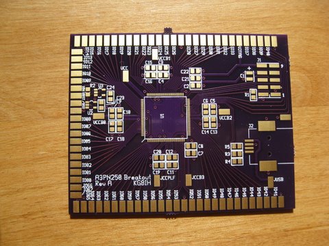
They came out quite nicely, with no obvious defects, and they look quite regal with gold plating and Laen’s signature purple solder mask. How often do you see purple circuit boards?  The gold is nice, too. Laen’s standard boards are have a solder finish, but sometimes some of his customers pay the extra for gold, in which case all the boards on that order come back with gold.

The FPGA board, gleaming and ready for some solder.

I’m looking forward to building up these boards and writing some Verilog to bring them to life.

No PCBs this week

I had hoped to be able to write about the new printed circuit boards this weekend, and maybe even show one built up, but they didn’t arrive. I had guessed that it would take them 9 days to get to Ohio from Oregon, which would have made them arrive yesterday.  There have been several snowstorms in areas they would be passing through, so it’s quite possible they were delayed by weather.

I’m still working on getting the Actel Microsemi development environment set up at home. When I tried to register for a free license key, the web site was down for maintenance.  I’m looking forward to getting it installed and starting work on some Verilog code. First up will be an iambic keyer.

FPGA Breakout Board Layout

Here at last is the printed circuit board layout for the FPGA breakout board. I’m planning a series of projects involving FPGA-based DSP for ham radio, and in order to build them, I need an FPGA and a PCB on which to mount it….

The goals for this layout constrained it to be a nearly single-sided layout, …

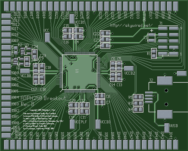
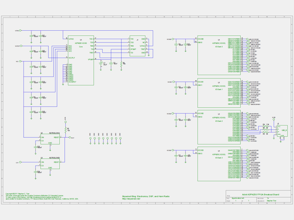
Here at last is the printed circuit board layout for the FPGA breakout board. I’m planning a series of projects involving FPGA-based DSP for ham radio, and in order to build them, I need an FPGA and a PCB on which to mount it. In the last installment of the project, I presented the schematic for the breakout board.

The goals for this layout constrained it to be a nearly single-sided layout, with a ground plane on the back. That way, the board could be mounted directly on a piece of copperclad with no short circuits to ground. My budget limited me to a double-sided board, so all signal and power traces had to go on the top side.

That said, here is the layout, top and bottom.

FPGA breakout PCB, top side

Continue reading “FPGA Breakout Board Layout”

FPGA Breakout Design Decisions

To get to my goal of a DSP-based ham radio using an FPGA as the DSP, I first need a way to prototype with an FPGA. Available FPGAs all use modern, small packages such as QFNs, QFPs, and BGAs. I can’t imagine soldering wires directly to a hundred tiny pins, so “dead-bug” construction, with the chip upside-down on a piece of copperclad board, is out. I need a breakout PCB that holds the chip and brings out its pins to something more reasonable to work with.

To get to my goal of a DSP-based ham radio using an FPGA as the DSP, I first need a way to prototype with an FPGA.  Available FPGAs all use modern, small packages such as QFNs, QFPs, and BGAs.  I can’t imagine soldering wires directly to a hundred tiny pins, so “dead-bug” construction, with the chip upside-down on a piece of copperclad board, is out.  I need a breakout PCB that holds the chip and brings out its pins to something more reasonable to work with.

Continue reading “FPGA Breakout Design Decisions”