Happy Birthday, Skywired!

Abstract first-order delta-sigma modulatorOne year ago today, I posted The Plan, the kickoff post both for this blog and for an ambitious DSP transceiver project. My wife had started a blog a few months earlier, and I was her sysadmin. I saw the fun she was having, and soon realized that administering two WordPress sites would not be much more work than administering one. The year since has brought 57 posts and pages about topics ranging from delta sigma data conversion to electronics books for children, but I’ve kept the project emphasis and the full-documentation style.

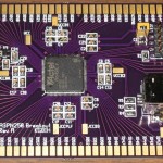
A3PN250 FPGA breakout boardThe transceiver vision from The Plan has shifted a bit. Initially, I planned an FPGA-centered design, even to the extent of building the analog-to-digital (A/D) and digital-to-analog (D/A) converters myself. That work led to a better understanding of delta sigma data conversion and with it a sense of realism about achievable levels of performance in a discrete design. I designed a high-performance A/D breakout board, but soon realized the pace of the project was likely to make me miss next year’s peak of the sunspot cycle and with it the best radio propagation for the next 11 years.

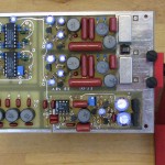
KK7B R2 receiver, top sideI changed my focus to building a transceiver around R2 receiver and T2 transmitter kits that are old enough to vote. That project is still in progress, by the way. The R2’s output amp isn’t working right yet.


The following pages were the most popular this past year:

  1. How to solder QFP, TSSOP, SOIC, and Other Surface Mount Parts
  2. A3PN250 FPGA Breakout Board
  3. The FPGA level shifter: Not entirely crazy!
  4. How Delta Sigma Works, part 1: Introducing the Delta Sigma Modulator
  5. How Delta Sigma Works, part 2: The Anti-Aliasing Advantage

Traffic has grown gradually but satisfyingly this year, bringing visitors from an even 100 countries. (The US is top, followed by the UK, Germany, Canada, and India.)

Thank you for reading. If you are a repeat visitor or an RSS subscriber, a big thank you for that as well. Here’s to more “Electronics, DSP, and Ham Radio”!

Have a great 2012!

Building a KK7B R2 phasing receiver

Hi, I’m back! It was a rough week, with a death in the family. As it ended, I found some time for some “solder therapy”. There is something good for the soul in putting together electronics. I don’t know if it’s the scent of the rosin or the satisfaction of seeing a project come together. All I know is it’s good for me.

KK7B R2 receiver, top side

The target of my soldering was my KK7B R2 receiver kit. This is the companion to the T2 I wrote about a few weeks ago. To my surprise, the R2 was easier to put together despite the higher part count. The components are larger, forcing a less dense pin matrix, and the board is separated into sections: mixers and diplexers, audio phase shift, low-pass filter, and audio amplifier. Conveniently, the board uses jumper wires (not yet installed on mine) to connect the sections. The intent appears to have been to make it easier to extend the board by swapping in a different phase shift network or adding alternate filters for CW or contesting, but it will make the board easier to debug as well, since I can bring it up a section at a time.

Keep in mind that this is a vintage kit that is no longer available, but updated versions of the design are still produced by Kanga US.

The board surprised me with its heft. I work mostly with surface-mount digital boards where the fiberglass PCB is the heaviest component. This board, though, weighs 134 g (4.7 oz), which is a lot for 100 cm2 (16 in2). The shielded inductors are the culprits. Each black cylinder in the photo is the ferrite shield of an inductor. Each inductor is noticeably heavy for its size, and this board has 10 of them.

KK7B R2 receiver board, bottom side

Once I wash the flux off (it’s not as much fun as soldering), the next piece of the puzzle is to build or buy a VFO. Rick, KK7B, designed a companion VFO for these boards, but it is out of production at the moment. I’m thinking about one of the Si570 VFOs out there. This little chip offers a very low phase noise synthesizer with tuning in steps of a fraction of a Hertz. Having this on a single chip was a pipe dream when the R2 and T2 were designed.

After that, I’ll need to build a power amplifier to boost the T2’s milliwatts up to a reasonable level — at least a watt, maybe as much as 50 W. Finally, I will have to integrate all the pieces into a working rig. Professionally, I do a lot of microcontroller work, so it’s tempting to build a fancy digital control panel with circuitry to integrate every R2 and T2 option imaginable. Instead, I’m trying to keep myself to something simple: one band, SSB only, and a digital frequency readout as the only frill.

I still have to pick the initial band. I’m torn between 20m, my favorite for PSK31, and 40m, which I like for SSB. I’m after whatever DX I can land in either mode. What band would you recommend?

Making a coax feedthrough window for my shack

One problem every ham faces is how to get his signal from inside, where the radios are, to outside, where the antennas are. A while back, I prototyped replacing a screen in my basement windows with a feedthrough panel. The prototype used hobby polystyrene sheets, which were easy to work with but far too flexible for the job. As the weather cooled, I removed it and closed the window, for fear some mice or other critters would find it a convenient way into our nice, warm house. Without a feedthrough, I had no way to use my antenna, so it was time to build a permanent version.

The window I chose is a typical basement window made of glass block, with a small section that opens.
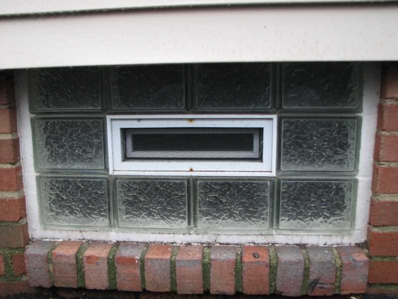
It didn’t take much work to remove the two screws that held the screen window.
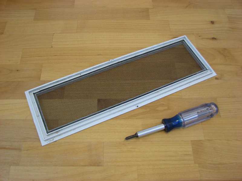
My plan was to cut a piece of acrylic (plexiglass) to replace the screen, but a friend one-upped that by giving me a piece of polycarbonate. This stuff is tough. A thicker version is used in bullet-proof windows! It will work fine for the job.

I put the screen on the polycarbonate for size.
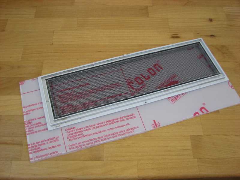
It’s perfect!

I marked the size I needed, along with the position of the screw holes, then used a scribing tool and a straightedge to scribe a deep line in the polycarbonate. The idea was to cut it like one cuts acrylic: by scribing it, then snapping it.
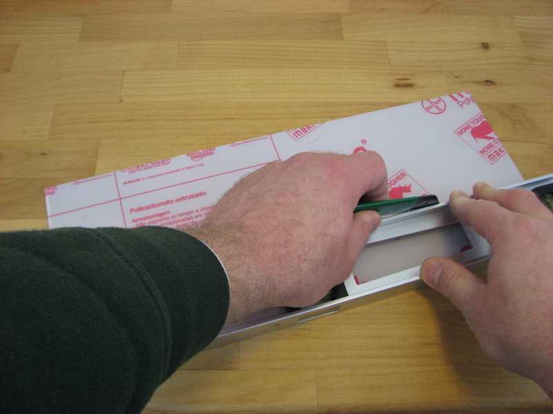
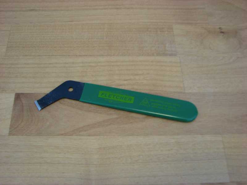
(This is what the plastic-scribing tool looks like. I found it in the window-repair section of my local hardware store.)
The polycarbonate was very hard to snap. I found out later that scribing and snapping is not the way to cut polycarbonate. In fact, it can shatter from this treatment. I should have cut it with a saw — I’m told table saws work particularly well.

In my ignorance, I scribed it deeper and deeper, trying to snap it over and over. Finally, it snapped. The material split a tiny bit along one edge (where the scriber had split and I had two parallel lines in the plastic), but in general the edge was clean and straight. I had scribed more than halfway through the sheet before it was ready to snap. Maybe I effectively sawed it after all…

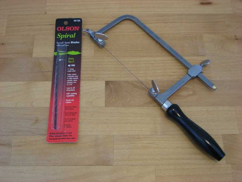
The next step was to make a hole for a BNC bulkhead feedthrough. The tool for this job was a jeweler’s saw with a spiral saw blade. These nifty blades are round and can cut in any direction without turning.
As a template, I used an electrical-box faceplate that had two holes for BNC feedthroughs like this. It came from the trash when an old coax-based (“thinwire”) Ethernet installation was upgraded to twisted pair.

I drilled the hole with my little Dremel drill press.  Some Googling of polycarbonate turned up recommendations against using a hand drill with it, because it can break bits if they aren’t held straight. I wish I had a real drill press, but this attachment for my Dremel tool seemed a good choice when I wanted to drill holes in homemade PCBs. It worked great for this job, too. A 1/8″ hole, the largest I had a collet for, was more than large enough to slip the saw blade through.
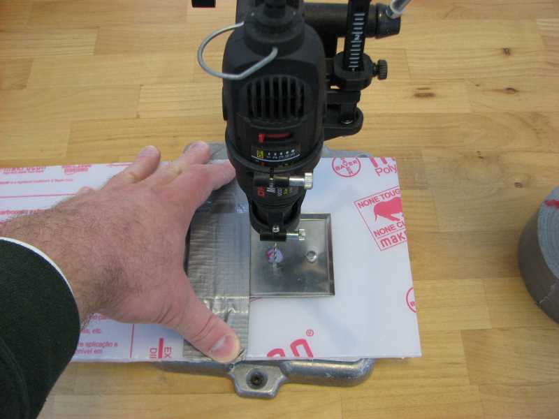
I also used the drill press to make two holes for the screws that will hold the panel in place.

As I sawed, I took care not to run the blade right against the template. It is stainless steel and would have dulled the blade much faster than the polycarbonate. In any event, I also had trouble turning one corner and needed to clean that up as well.

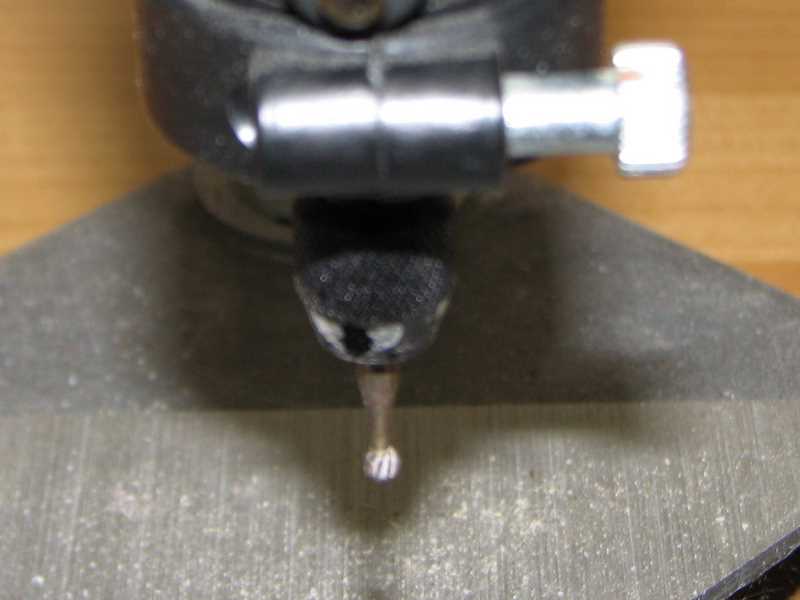
I set up the Dremel with my favorite burr bit, which looks like it needs to be replaced soon. It went through the polycarbonate like butter, quickly bringing the edges of the hole out to match the template.
I removed the template and tried the BNC bulkhead feedthrough for size. It fit perfectly! My past includes many a panel with misshapen holes that barely fit their intended connector, so this was surprising but welcome. I guess that’s what I get for never using a template before. The feedthrough I used was the former resident of the faceplate-turned-template.
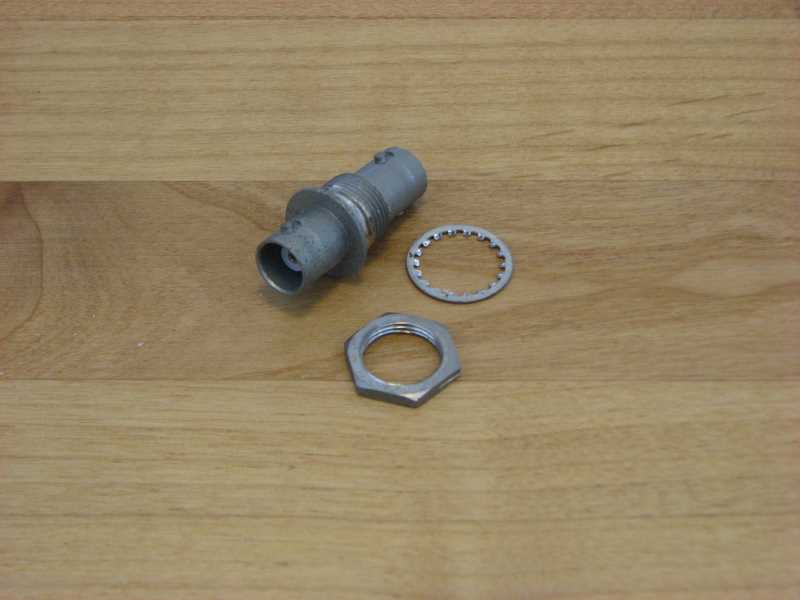
Now, one thing to mention here… I took care to put the nut on the inside of the panel. I used Coax-Seal on the outside connection, to prevent water ingress, and that stuff is messy and a bother to remove and replace. By putting the nut on the inside, I can remove and replace the feedthrough window without disturbing the Coax-Seal. That might be handy when I cut a hole for another connection.

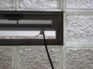
Finally, I put it all together. I pulled the protective covering off of the polycarbonate, installed the feedthrough for real, and screwed it in place of the screen window. It was a little dusty, so I cleaned it before I installed it. Now it is so clear that the coax looks like it floats in space.
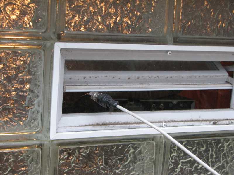
The clearance between the internal, movable window and the feedthrough window is enough that I can close the window after disconnecting the internal coax. (I figured that out with the polystyrene prototype.) That’s good for energy efficiency. The panel fits tightly enough that I don’t feel a draft, and I could always add weather stripping, but it’s still only a single-paned window. The moveable window behind it is double-paned.

The picture above shows the Coax-Seal, too. My technique for that, which I learned from the hams at the Case Amateur Radio Club, is to first wrap the connection with electrical tape, with the outer end folded over a bit to make a pull tab. Cover the tape with Coax-Seal, with the Coax-Seal extending a bit past the tape on each end for water-tightness. When you want to remove the connection, you can cut almost all the way through the Coax-Seal with a sharp knife, split the rest open like peeling an orange, and remove it down to the electrical tape. Next, unwrap the tape started at the pull-tab. The tape will take the perpetually sticky Coax-Seal residue with it, leaving a clean pair of connectors ready for reuse.

Jay Eiger was a font of wisdom for this project and also gave me the polycarbonate. Thanks, Jay!
Itead Studio’s Open PCB exchange: how it worked out

The boards I ordered last month from Itead Studio arrived with something extra: someone else’s boards! No, it was not a mistake, but a 10-cent option that I could not resist: the Open PCB service. For 10 cents above the cost of a prototype PCB order, Itead fabbed two extra boards of my design. Those boards went into a pool of boards from the other Open PCB participants, then Itead sent each of us two random boards from the pool. All participating boards are supposed to be open source. Sure, there is no guarantee that the boards will be at all useful to the recipient, but who knows, maybe something nifty will arrive!

I ordered the Open PCB option with my AK5388 ADC board. Along with my 8 copies of the board, I received two boards from strangers. Both are 5 cm x 5 cm, which is likely a popular size for Itead because it’s the maximum size for their cheapest PCB fab deals.

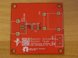
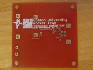
Boston University Rocket Team thermocouple digitizer PCB, top side Rocket team's thermocouple digitizer PCB, bottom side

The first board is a thermocouple digitizer from the Boston University Rocket Team. The team has posted the schematics, layout, and Gerbers online on GitHub. The board was clearly labelled, making it easy to find the documentation in Google. It even had a QR code. though the pixels were blurred by the silkscreen and my phone was unable to read it. It’s a great idea for open source hardware, though, and would probably work if it were a little bigger.

The design uses a single MAX31855 as a thermocouple-to-digital converter. This is a neat chip that contains a thermocouple amplifier, cold-junction compensation, and a 14-bit ADC all in an 8-pin SOIC. That’s a ton of analog circuitry condensed into a single chip! It can cover temperatures from near absolute zero to molten metal, with quite respectable accuracy and resolution.  The board runs the chip’s Serial Peripheral Interface (SPI) to a USB 3 connector, wired in a non-standard way that carries power (12V, 5V, and 3.3V) and an SPI bus.

The Rocket Team has chosen an interesting mission. They don’t fly rockets, but rather research the design and performance of hybrid rocket motors, including firing them on a static test stand. They build their own instrumentation, all open source hardware, and this board is part of that package. I can see why they would be interested in accurately measuing the temperature of very cold and very hot things!

The board actually has some potential to be useful to me. I don’t need a thermocouple interface right now, but I can imagine using for one down the road to monitor a reflow oven or to manage the heatsink temperature in a linear amp.

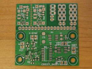
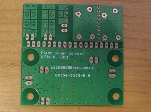
Ville K's board, top side  Ville K's flash power control board, bottom side

The second board is a bit of a mystery.

On first inspection, I was puzzled by the single-row header right across the middle and the smaller row of holes at the upper-left side. Eventually I noticed that there are no traces running to either, so it’s likely that they are perforations to simplify cutting the board into three pieces.

The bottom portion is the least obscure. It bears the labels “Flash power control” and “X-SYNC”, so it must have something to do with photo flash. Beyond that, I’m stumped. A two-pin header for an IGBT (a three-terminal device) particularly leaves me scratching my head. The designer did a nice job of bonding his top-side ground pour to the bottom-side ground plane with plenty of vias, including all around the edge of the board.

On the upper right, there are two copies of a circuit, separated by a row of holes to aid breaking them apart. The circuit has a transistor in SOT-23, a diode, a few capacitors, a resistor, and what is likely an IC in a small 5-pin package. Looking at the topology, I think the circuit is a boost converter, at least if the unlabeled two-pad component on the center left is an inductor.

The patterns in the upper right corner are even harder to understand. They look like series chains of something, maybe resistors or LEDs. The vias in the pads and the wide traces indicate that the designer was concerned about resistance, inductance, or heat dissipation. Since the three-device chain (upper center of the board) has the triple vias to back-side copper, but does not use the copper to interconnect, I would guess heat sinking is the concern. It could be a challenge to reflow the board with the open vias in the pads, but it’s probably meant to be hand-soldered. When hand-soldering, one can keep feeding solder until the holes have wicked up their fill.

I sent some e-mail to the address in the silkscreen but got no reply. Google searches on other likely terms turned up nothing. I’m left with a board and guesses.

The Open PCB  exchange is a great idea, and I’ll happily participate again in the future. The thermocouple board is an example of how it can go right. I got a well-documented board that led me to find out about the Rocket Team’s interesting work. In contrast, the Flash Power Control board is an example of what can go wrong. There is nothing to stop someone from entering an undocumented PCB in the exchange, getting documented and interesting boards but failing to repay the favor. Still, I like seeing what other people are doing and hopefully two other people enjoyed seeing what I’m up to. For 10 cents, less than a 1% increment on the cost of a PCB order, it’s worth it.

Have you tried Open PCB, and how did it work out? Are you able to shed any light on the mystery board?  As always, comments are welcome!

Building a KK7B T2 phasing transmitter

Are you the kind of tinkerer who has a few unbuilt kits sitting around?  I mentioned last week that I want a faster way to get on the air than a designed-from-scratch SDR. If I stick to my current course, I may miss the peak of this solar cycle.  It turns out that I have had an R2 receiver and a T2 transmitter kit on hand for… well, a very long time. If I recall, I bought them as soon as they were available in 1994.

These are very neat radios. Rick Campbell, KK7B, set a goal of pushing the state of the art in direct-conversion receivers. His series of high-performance receivers includes the R1, R2, R2pro, miniR2, microR2, and microR1. The R2 family are single-signal direct-conversion receivers, and the T2 and microT2 are companion transmitters.

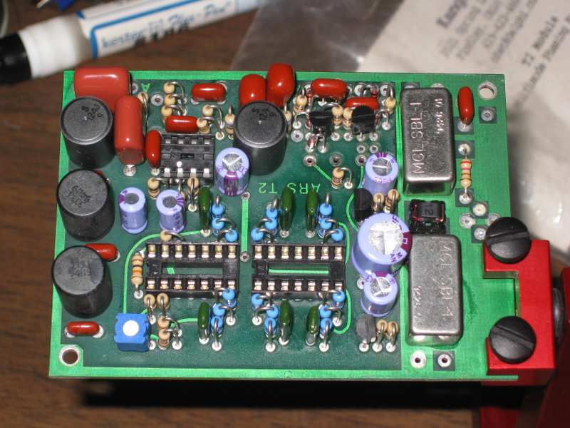
KK7B T2 exciter, top side

The T2 uses the phasing technique to generate single sideband. In this technique, the audio signal is passed through a filter (or a pair of filters) that generate two signals 90 degrees out of phase. These are mixed with local oscillator (LO) signals that are also 90 degrees out of phase. When the mixer products are summed or subtracted, a miracle of trigonometry occurs, producing a clean single-sideband signal.  As long as both sides of the system have closely-matched gains and the 90 degree phase shifts are very accurate, the opposite sideband is suppressed by 40 dB or more.

I decided to build the T2 first. Rick’s layout style is very dense, and I wanted to try the board with fewer components first. These are through-hole boards with the component holes falling on an 0.1″ grid in both directions. With only two exceptions, all of the resistors and diodes are installed “standing up”, with their leads 0.1″ apart and 0.1″ spacing to neighboring parts. The T2 board has no silk-screen, making construction that much more challenging. In any event, a fine-tipped iron and small-diameter solder (I chose 0.025″) are the tools of the day.

Rick suggests stuffing all of the parts before soldering any, as a hedge against putting them in the wrong holes. Then he recommends soldering and trimming the leads in rings from the outside in. I tried thaat, and it worked OK. For the R2, I will probably mount some of the trickier components individually, then switch to Rick’s method for the rest.

As you might expect, I had a few problems with solder bridges, but nothing a little solder wick couldn’t clean up.

Although there was no visible tarnish on this 17-year-old board, I did notice that the solder didn’t wet the pads as well as usual. Eventually I thought to start adding flux with the flux pen that I use for surface-mount work, and that did the trick.

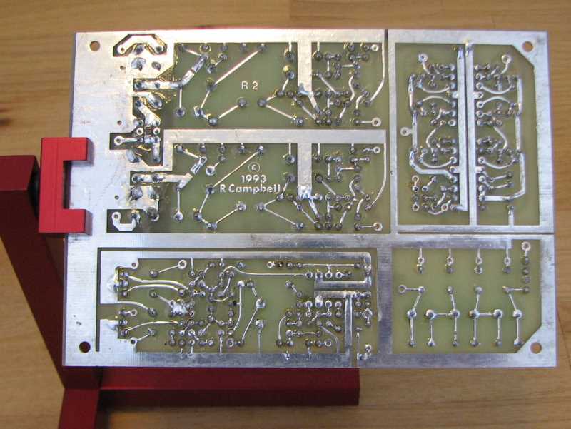
Here is my handiwork. I’d like to solder as beautifully as Tom, the electronics tech I work with, but for basement tinkering this will suffice.

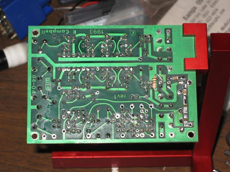
KK7B T2 phasing SSB transmitter, bottom side

The T2 needs one more once-over for bridges and cold joints, then I’ll apply power and see what happens!

Links:

Building the AK5388 ADC breakout board

“Honey, the package you’ve been waiting for from Hong Kong is by your computer,” said my dear wife shortly after I got home from work on Friday. Even better, a few minutes later she suggested that I spend the evening in the basement, building up one of my new boards. I have a wonderful wife!
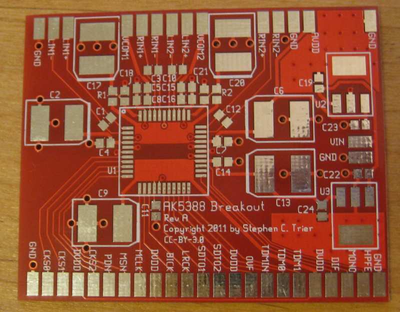
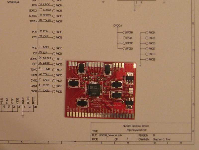
The AK5388 ADC breakout boards finally arrived!  I had a hard time waiting for them. First, Itead Studio didn’t ask me to correct the design until the day the finished boards were supposedly going to ship. (They did apologize for the delay — it sounded like there was a communications snafu between them and the fab.) Then I waited five more days for the board to be fabbed. Shipping from Hong Kong to Ohio took ten days. Looking around on the web, I’ve seen shipping times reported from seven to ten days, sometimes going up to as much as 20 days during the holiday season.

All eight boards look great. Other people who tried Itead reported some over-etching and silkscreen problems, but I don’t see any defects on mine. Since Itead now does 100% electrical testing, I have confidence that the boards will all work. I could spot the tiny dimple in each pad where the flying probes touched down, so it is clear that all eight boards were tested.

I went to the basement and heated up the soldering iron. The board went together easily. The 0.80 mm pitch of the AK5388 was downright easy to solder after the 0.50 mm  A3PN250 FPGA and other fine-pitch parts I’ve been using at work. Besides, I’ve learned some new soldering techniques lately that helped me solder the AK5388 quickly, but I’ll have to share those in another post. I did use a meter to check all of my AK5388 solder joints, though. There were a few bridges, but they cleaned up without a problem.

The pads for the big electrolytic capacitors are larger than necessary. I used PCB’s default EIA7343 footprint. The pads had plenty of room for the soldering iron, but they could have been smaller without sacrificing ease of assembly. (Did I use the wrong footprint once again? 0805 capacitors seem to be the only ones I get along with…)

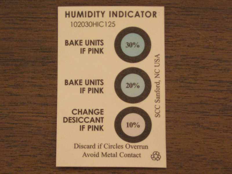
Lately Digi-Key has been taking much stronger steps to control moisture uptake by the semiconductors they sell. Instead of just shipping some cut tape in an anti-static baggie, they now seal the chips in an airtight bag with a packet of dessicant and a humidity indicator. I opened the bag this one was in about 4 weeks ago. Not bad so far, considering it was in my not-very-dry basement that whole time. Moisture uptake is important for reflow soldering techniques, but as far as I can tell, it is less significant for hand-soldering.

Now I’m left asking myself what comes next. In my original plan, the next step was to couple the ADC to the FPGA, put a USB core on the FPGA, and build a sound card. Once that works, adding a local oscillator and a quadrature mixer will make everything I need for a PC-based software-defined-radio (SDR) receiver, and this long trek will finally result in a radio.

However, I hear that the bands are great these days, and I’m not sure I want to take the time to homebrew an SDR rig just to get on the air. Maybe I should spend some time on a faster route to a radio, then come back to the SDR. I’ll probably have more on that idea next week.

Until then, keep on tinkering, and as always, your comments are welcome!

Trying out Itead Studios’s PCB prototyping service

I’m working on building a breakout board for the high-performance AK5388 audio ADC. In my last post, I revised the schematic to help with the PCB layout and test-fit the key components on a printout of the board.

The next step was to order the board. Laen’s PCB order is taking a hiatus this month. Feeling impatient, I decided to try one of the Chinese options: Seeed Studio’s or Itead Studio’s PCB fab services. They offer prices as low as $9.95 for 10 copies of a 5 cm x 5 cm board. Unfortunately, the ADC board is 4.9 cm x 6 cm. That extra centimeter nearly doubled the cost of the board, because I had to buy a 5 cm x 10 cm package. At least one dimension was still below 5 cm!

My son wandered in while I was comparing prices. He asked, “Is your circuit board going to be purple?”  I told him that no, it was probably going to be green.  “I think it should be red!” he said.  “What the heck,” I thought, and clicked on the button for Itead’s color PCB service. The deal was $23 for 8 boards. That compares with $18 for 10 boards if they are green. Since both 8 and 10 boards are more than I need, it’s basically $5 extra for the custom color. I went for it.

For what it’s worth, one difference between Itead and Seeed is that Seeed only offers 50% electrical testing for their base prices, with 100% testing costing more. Itead has 100% e-test with their base prices. Itead and Seeed are having a bit of a price war over these PCB services, so their offers may well have changed by the time you read this.

Itead is offering an interesting bonus deal with their PCB services: PCB sharing. For a token 10 cents above the cost of the PCB service, they will send me two random boards from other designers. In exchange, they will send two additional copies of my board to other sharing participants. There is no guarantee the boards will be remotely useful to the recipient, but for 10 cents, how could I resist?

(By the way, if you’re reading this because you saw the skywired.net URL on a board Itead sent you, please drop me a note! I’d love to hear who you are and what you’re working on.)

I expected roughly a five day turnaround from Itead, and was disappointed when after five days, I received an e-mail that the fab had rejected my Gerber files. Itead wants the board outline on at least one Gerber layer. Now, both Laen and Sparkfun’s BatchPCB accepted the groundplanes on my boards as the outline, so I didn’t expect trouble from Itead. However, they were certainly within their rights to ask me for a correction. It was quick to add it, and a few hours later they told me my new Gerbers had been sent to the fab.

I’m still waiting for the PCBs, which were shipped Wednesday. Now I have to wait for them to come by airmail from Hong Kong. It’s hard to be patient!