An enclosure for the R2/T2 transceiver

After months of organizing parts, I have finally gotten back to the R2/T2 transceiver project. Don’t get me wrong, the cleaning and sorting is not done, but I felt the urge to do something a bit more… constructive.

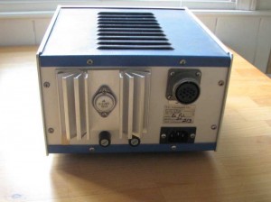
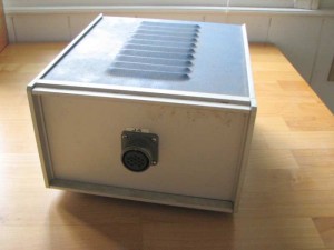
While cleaning, I found a box of old electronics junk that had promising cases. Electronics enclosures are expensive. Salvage can be a good way to keep the cost down. I don’t know what this thing once was, but there are military-style circular connectors on the front and back, two fuse holders, a power inlet, and no visible controls.


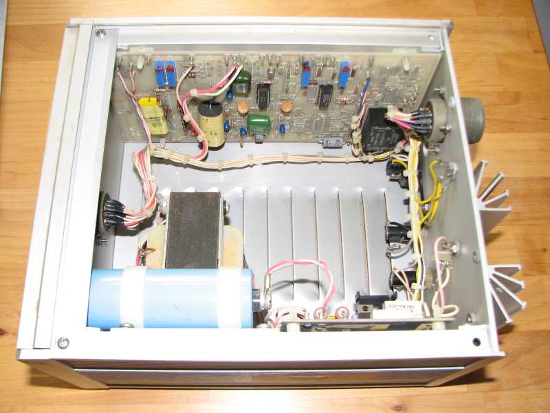
Opening it up, I found this:

There’s a lot of empty space in there! It looks like it was some kind of power supply. Next to the weighty transformer and big blue filter cap, a circuit board carried 7805 and 7806 regulators, several current-sense resistors and an LM324 quad op amp. It also had a power transistor on board and connected to the big TO-3 transistor on the heat sink in the back.

The board on the other side had a couple of high-voltage film capacitors, some ten-turn pots with their positions set with nail polish, two LM324’s and one RCA 4151 voltage-to-frequency/frequency-to-voltage converter. Down in the lower-right corner, it also held a solid-state relay. I’m a little more stumped about what this board was for. Maybe it was more power-supply logic, or maybe some kind of controller.

Tracing out the wiring harness revealed that 120VAC is run to the front connector, with only a fuse between the connector and the power cord. That could get exciting quickly to anyone not expecting it.

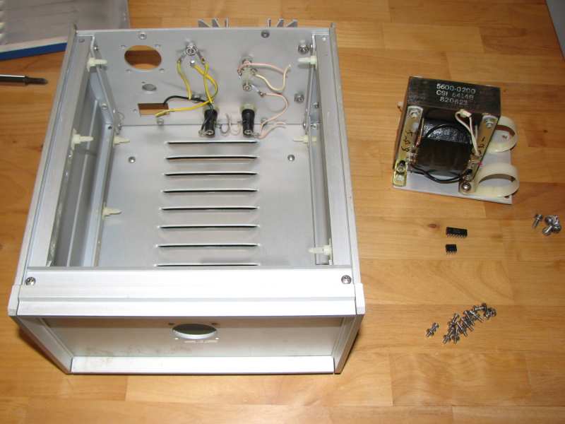
I pulled apart the whole thing, salvaging only the transformer, two ICs, and some fasteners. I tried to salvage all the ICs, but some were corroded into their sockets and could not be extracted without breaking pins. I have not had that happen before.

That’s the final product. I left the fuse holders, the heat sink, and a common ground point in place. They might be useful when this box becomes a transceiver. The front and back panel are 0.125″ aluminum and slide out after a few screws are removed. It will be easy to replace them with new panels for the radio.

The only fixed surfaces in this box on which to mount things are a pair of narrow rails on each of the side extrusions. The bottom is removeable and isn’t set up well to hold circuit boards. I will have to either add a false bottom or come up with a way to mounting the boards at right angles from the sides. Putting the boards flat on the sides, like the original residents of this box, won’t give me enough room, and because the boards are not sized to fit the walls, I would have to improvise some kind of mounting panel or angled standoffs to hold them anyway.

In any event, that problem is solvable. It’s a nice case for what I hope will be a nice radio.
SMT Soldering – It’s Easier Than You Think

Front page of "SMT Soldering: It's Easier Than You Think"Soldering Is Easy was a great starter, and now here’s a sequel: SMT Soldering – It’s Easier Than You Think.  Greg Peek and Dave Roberts put together a great little comic book that teaches the art of soldering tiny SMT components. After reading it, you will be ready to tackle chip resistors, SOT-23’s, and SOIC’s with confidence.  (You might also like to take a look at Skywired’s own tutorial on soldering SMT ICs.)

The comic book is licensed CC-BY-SA (Creative Commons Attribution Share Alike), so everyone is free to pass it on.

(Via MightyOhm.)

KK7B R2 receiver: lifted pads, a scorched board, and it works anyway

I’m slowly making progress on my KK7B R2/T2 transceiver project. At my last report, I was waiting for replacement capacitors to arrive. They did, and I pulled out my ancient solder-removal iron, a Radio Shack unit from who knows how long ago.

Either my unsoldering skills are rusty or I was too impatient, or both. I managed to lift four pads, completely demolishing one. The other three were salvageable. I’d like the board to be perfect, but having it work is an acceptable substitute.

The new caps went in easily, with only a little fiddling to wire around the ruined pad. Better yet, the excessive bias current I saw before the replacement is gone! The board is supposed to be adjusted to 100 mA current. It used to start at 120 mA, with the bias adjustment set to its minimum, and drift its way up to more and more current from there (going as high as 200 mA before I’ve lost my nerve and switched it off). Now it starts at 84 mA and… drifts its way up from there to 130 mA and more.

OK, so one problem was solved. I can always increase current with the bias adjustment potentiometer.

After scratching my head a bit, I finally noticed one small sentence in KK7B’s articles on the R1 and R2. The audio output transistors need a heat sink, do they? Oops! I dug around a bit in my junk box but couldn’t find anything that would fit. The articles say the audio amp will drive a pair of headphones fine without the output transistors, so I decided to take them out.

I recently got a Sparkfun hot-air soldering station (a Sparkfun Free Day prize!) and thought I’d give it a shot. Sure, hot air is usually for surface-mount parts, but solder is solder, right?  Not being sure how to set the airflow and temperature settings, I set both on the high side, put some flux on the output transistors’ pads, and went for it. The result wasn’t pretty:

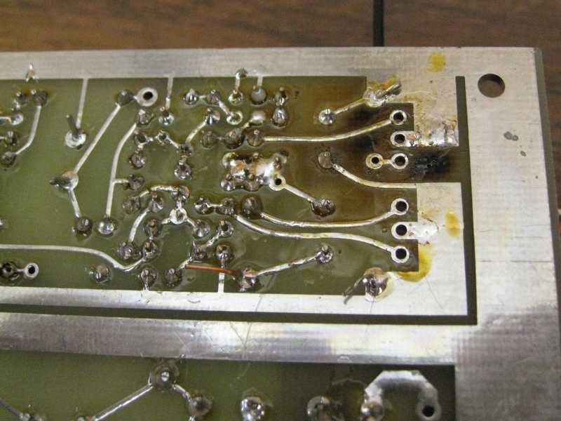
Oops... A scorched R2 PCB

Yes, I scorched the board. Oops. Between this and the lifted pads, I think I need to work on my unsoldering skills.

Since the transistors are 50 cent parts (TIP29/TIP30), I unsoldered them the easy way: I cut the leads, removed the leads from the board with my conventional iron, then cleaned out the holes with my solder sucker. I didn’t damage any pads this time!  (The picture above was taken after all of these steps.)

A little more soldering to hook up a BNC and some other goodies, and the board was alive!

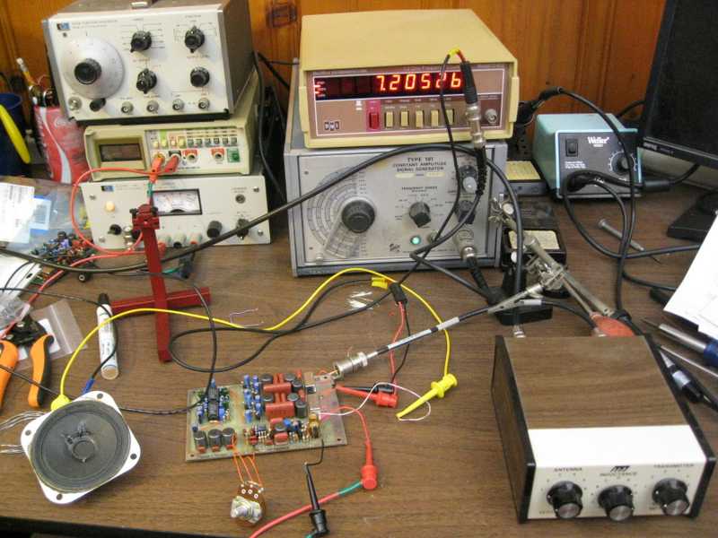
R2 on the bench, surrounded by test equipment

That’s a Tek 191 signal generator as the VFO (variable frequency oscillator), with a frequency counter as the readout. That’s an MFJ QRP antenna tuner in the foreground.

I didn’t build a phasing network yet, so I drove only one VFO input. That causes the R2 to function like a conventional direct-conversion receiver,receiving both sidebands simultaneously. That said, it works. I was able to hear signals, though frankly many were quite hard to copy. I’m not sure what else might be wrong.

The frequency counter spits out a lot of digital noise. I learned to flip it on only to spot-check my frequency. It’s a lot quieter in standby mode.

Did I mention that IT WORKS?

Despite the success, I’ve been struck by a bit of paralysis in moving forward. There are so many choices to make for integrating the radio.

  • What kind of VFO should I use? Should I design my own or buy a kit?
  • Which modes should I include?
  • How much power output do I want?
  • What power amp should I use? Should I design my own or buy a kit?
  • Which case should all of this go in?
  • What microphone, and microphone connector, should I plan for?

Keep in mind that this is supposed to me my fast route to getting on the air, so I’m thinking kits for both the VFO and amp. Besides, with as busy as it has been at work lately, it is nice to sit back and just build something.

It’s not a pretty project any more, but it works! Hooray!

Building a KK7B T2 phasing transmitter

Are you the kind of tinkerer who has a few unbuilt kits sitting around?  I mentioned last week that I want a faster way to get on the air than a designed-from-scratch SDR. If I stick to my current course, I may miss the peak of this solar cycle.  It turns out that I have had an R2 receiver and a T2 transmitter kit on hand for… well, a very long time. If I recall, I bought them as soon as they were available in 1994.

These are very neat radios. Rick Campbell, KK7B, set a goal of pushing the state of the art in direct-conversion receivers. His series of high-performance receivers includes the R1, R2, R2pro, miniR2, microR2, and microR1. The R2 family are single-signal direct-conversion receivers, and the T2 and microT2 are companion transmitters.

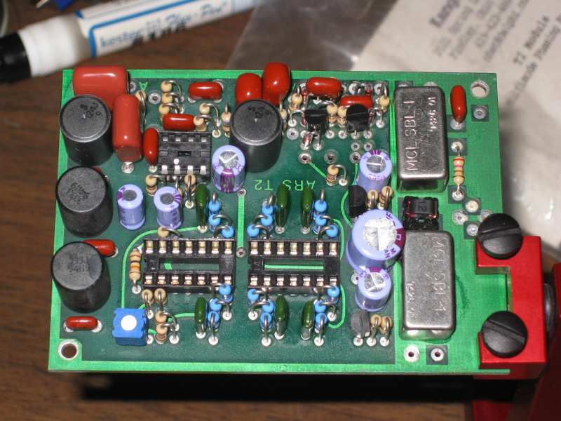
KK7B T2 exciter, top side

The T2 uses the phasing technique to generate single sideband. In this technique, the audio signal is passed through a filter (or a pair of filters) that generate two signals 90 degrees out of phase. These are mixed with local oscillator (LO) signals that are also 90 degrees out of phase. When the mixer products are summed or subtracted, a miracle of trigonometry occurs, producing a clean single-sideband signal.  As long as both sides of the system have closely-matched gains and the 90 degree phase shifts are very accurate, the opposite sideband is suppressed by 40 dB or more.

I decided to build the T2 first. Rick’s layout style is very dense, and I wanted to try the board with fewer components first. These are through-hole boards with the component holes falling on an 0.1″ grid in both directions. With only two exceptions, all of the resistors and diodes are installed “standing up”, with their leads 0.1″ apart and 0.1″ spacing to neighboring parts. The T2 board has no silk-screen, making construction that much more challenging. In any event, a fine-tipped iron and small-diameter solder (I chose 0.025″) are the tools of the day.

Rick suggests stuffing all of the parts before soldering any, as a hedge against putting them in the wrong holes. Then he recommends soldering and trimming the leads in rings from the outside in. I tried thaat, and it worked OK. For the R2, I will probably mount some of the trickier components individually, then switch to Rick’s method for the rest.

As you might expect, I had a few problems with solder bridges, but nothing a little solder wick couldn’t clean up.

Although there was no visible tarnish on this 17-year-old board, I did notice that the solder didn’t wet the pads as well as usual. Eventually I thought to start adding flux with the flux pen that I use for surface-mount work, and that did the trick.

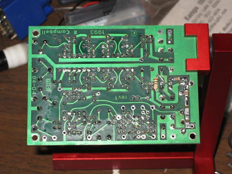
Here is my handiwork. I’d like to solder as beautifully as Tom, the electronics tech I work with, but for basement tinkering this will suffice.

KK7B T2 phasing SSB transmitter, bottom side

The T2 needs one more once-over for bridges and cold joints, then I’ll apply power and see what happens!

Links:

Building the AK5388 ADC breakout board

“Honey, the package you’ve been waiting for from Hong Kong is by your computer,” said my dear wife shortly after I got home from work on Friday. Even better, a few minutes later she suggested that I spend the evening in the basement, building up one of my new boards. I have a wonderful wife!
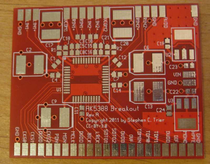
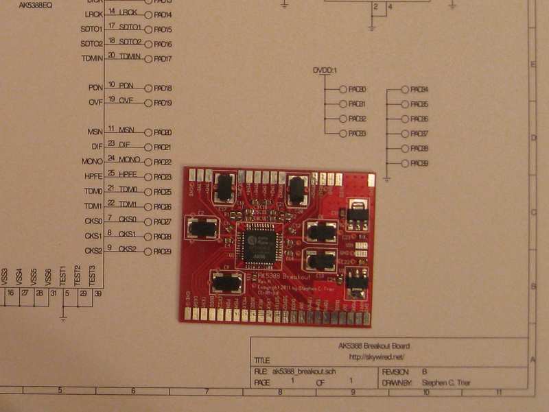
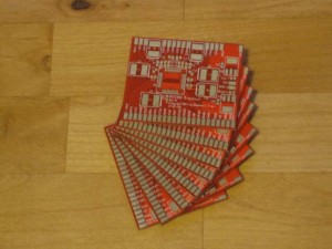
The AK5388 ADC breakout boards finally arrived!  I had a hard time waiting for them. First, Itead Studio didn’t ask me to correct the design until the day the finished boards were supposedly going to ship. (They did apologize for the delay — it sounded like there was a communications snafu between them and the fab.) Then I waited five more days for the board to be fabbed. Shipping from Hong Kong to Ohio took ten days. Looking around on the web, I’ve seen shipping times reported from seven to ten days, sometimes going up to as much as 20 days during the holiday season.

All eight boards look great. Other people who tried Itead reported some over-etching and silkscreen problems, but I don’t see any defects on mine. Since Itead now does 100% electrical testing, I have confidence that the boards will all work. I could spot the tiny dimple in each pad where the flying probes touched down, so it is clear that all eight boards were tested.

I went to the basement and heated up the soldering iron. The board went together easily. The 0.80 mm pitch of the AK5388 was downright easy to solder after the 0.50 mm  A3PN250 FPGA and other fine-pitch parts I’ve been using at work. Besides, I’ve learned some new soldering techniques lately that helped me solder the AK5388 quickly, but I’ll have to share those in another post. I did use a meter to check all of my AK5388 solder joints, though. There were a few bridges, but they cleaned up without a problem.

The pads for the big electrolytic capacitors are larger than necessary. I used PCB’s default EIA7343 footprint. The pads had plenty of room for the soldering iron, but they could have been smaller without sacrificing ease of assembly. (Did I use the wrong footprint once again? 0805 capacitors seem to be the only ones I get along with…)

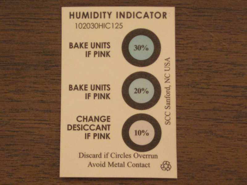
Lately Digi-Key has been taking much stronger steps to control moisture uptake by the semiconductors they sell. Instead of just shipping some cut tape in an anti-static baggie, they now seal the chips in an airtight bag with a packet of dessicant and a humidity indicator. I opened the bag this one was in about 4 weeks ago. Not bad so far, considering it was in my not-very-dry basement that whole time. Moisture uptake is important for reflow soldering techniques, but as far as I can tell, it is less significant for hand-soldering.

Now I’m left asking myself what comes next. In my original plan, the next step was to couple the ADC to the FPGA, put a USB core on the FPGA, and build a sound card. Once that works, adding a local oscillator and a quadrature mixer will make everything I need for a PC-based software-defined-radio (SDR) receiver, and this long trek will finally result in a radio.

However, I hear that the bands are great these days, and I’m not sure I want to take the time to homebrew an SDR rig just to get on the air. Maybe I should spend some time on a faster route to a radio, then come back to the SDR. I’ll probably have more on that idea next week.

Until then, keep on tinkering, and as always, your comments are welcome!

Soldering is Easy comic book is now in 12 languages

Soldering Is Easy cover, English versionThe Soldering is Easy one-page comic has grown to an eight-page comic book, and it’s available in 12 languages! Mitch Altman, Andie Nordgren, and Jeff Keyzer created the original, and the translations were done by volunteer translators. It’s a great idea and well worth a read.

Here is every translation so far, all from Jeff’s MightyOhm blog:

Soldering is Easy (English)

ПАЯТЬ ПРОСТО (Russian)

Soldering is Easy (Simplified Chinese)

Solder É Fácil (Portuguese)

Menyolder Itu Gampang (Indonesian)

Soldar es Fácil! (Spanish)

… — .-.. -.. . .-. .. -. –. .. … . .- … -.– (Morse code)

Soldering is Easy (Japanese)

Οδηγός Για Εύκολη Συγκόλληση (Greek)

Löten ist einfach (German)

Souder c’est Facile (French)

Soldering is Easy – Traditional Chinese

Lutowanie Jest Proste (Soldering is Easy – Polish Translation)

Thanks, Mitch, Andie, Jeff, and translators for your great work!

Making progress on the A3PN250 FPGA breakout…

I’ve made lots of small steps on the A3PN250 FPGA breakout board the last two weeks.

Firstly, I built an JTAG adapter cable to work around a wiring error on the PCB. When I laid out the board, I accidentally numbered the pins on the JTAG connector DIP-style instead of ribbon cable style.  That meant that all the pins except for pin 1 were wired wrong. After thinking a bit about the options, which included scrapping the board and starting over, or skywiring in corrected wiring for the connector, I decided the cleanest solution was to make a custom JTAG cable that moved the pins around where they belong. I’d seen other cables built this way. I asked myself, “How hard could it be?” Continue reading “Making progress on the A3PN250 FPGA breakout…”