The FPGA level shifter: not entirely crazy!

Some months ago, I came across an Actel app note that advocated using FPGAs as level shifters. “What a crazy waste of computing power,” I thought to myself, “though I suppose they are just trying to sell the low-end ProASIC3 nano FPGAs.” With that, I set the thought aside.

Much later, I ran into a problem.

Some months ago, I came across an Actel app note that advocated using FPGAs as level shifters. “What a crazy waste of computing power,” I thought to myself, “though I suppose they are just trying to sell the low-end ProASIC3 nano FPGAs.”  With that, I set the thought aside.

Much later, I ran into a problem. I had a prototype board to design. It had to plug into an existing, quite complicated microprocessor evaluation kit, adding a data radio and a few other functions to the system. After poring over the schematic for hours, the software developer, who I’ll call S, and I still weren’t 100% sure which pins on the expansion bus were free for our use, though we had a long list of pins that definitely were not suitable. On top of that, I had a level-shifting problem. The evaluation kit ran at 1.8 V and 2.75 V, with signals at both levels on the bus, but the radio required 3.3 V logic levels. Continue reading “The FPGA level shifter: not entirely crazy!”

How Delta Sigma Works, part 1: Introducing the Delta Sigma Modulator

Today I’d like to turn to the fascinating topic of delta-sigma techniques. Delta-sigma is best known for its use in analog-to-digital and digital-to-analog converters, but it also has a potent role in digital signal processing and even in analog applications. By its nature, delta-sigma can reduce the amount of analog circuitry needed in a radio or other electronics, and what is left is often simpler and cheaper than what would otherwise be required.

Beyond that, delta-sigma techniques are nifty! The core concept is counter-intuitive at first glance, yet it offers all kinds of powerful applications.

This post is part of a series on delta-sigma techniques: analog-to-digital and digital-to-analog converters, modulators, and more. A complete list of posts in the series are in the How Delta-Sigma Works tutorial page.

Today I’d like to turn to the fascinating topic of delta-sigma techniques. Delta-sigma is best known for its use in analog-to-digital and digital-to-analog converters, but it also has a potent role in digital signal processing and even in analog applications. By its nature, delta-sigma can reduce the amount of analog circuitry needed in a radio or other electronics, and what is left is often simpler and cheaper than what would otherwise be required.

Beyond that, delta-sigma techniques are nifty! The core concept is counter-intuitive at first glance, yet it offers all kinds of powerful applications. Working at understanding delta-sigma techniques gives deep insights to many other areas of signal processing.

This is the first of a multi-part series on delta-sigma, which is too broad and deep a topic to cover in a single post. There will be some math, balanced with an intuitive approach to the circuits. I will also delve into the the practical, building delta-sigma data converters and sharing the schematics and results. I will be learning about delta-sigma along with you, so stay tuned for more in future posts.

The place to begin is with a first order delta-sigma modulator, which is the simplest variety of delta-sigma circuit. A first-order modulator has a structure like this:
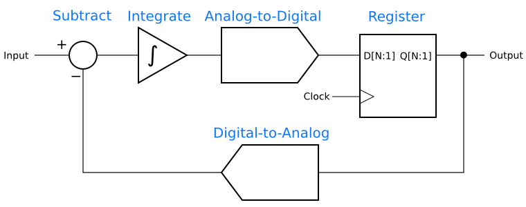
Abstract first-order delta-sigma modulator

Continue reading “How Delta Sigma Works, part 1: Introducing the Delta Sigma Modulator”

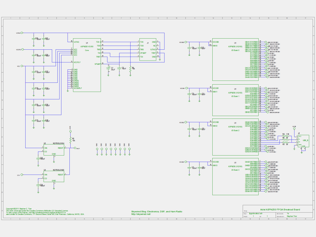
FPGA Breakout Design Decisions

To get to my goal of a DSP-based ham radio using an FPGA as the DSP, I first need a way to prototype with an FPGA. Available FPGAs all use modern, small packages such as QFNs, QFPs, and BGAs. I can’t imagine soldering wires directly to a hundred tiny pins, so “dead-bug” construction, with the chip upside-down on a piece of copperclad board, is out. I need a breakout PCB that holds the chip and brings out its pins to something more reasonable to work with.

To get to my goal of a DSP-based ham radio using an FPGA as the DSP, I first need a way to prototype with an FPGA.  Available FPGAs all use modern, small packages such as QFNs, QFPs, and BGAs.  I can’t imagine soldering wires directly to a hundred tiny pins, so “dead-bug” construction, with the chip upside-down on a piece of copperclad board, is out.  I need a breakout PCB that holds the chip and brings out its pins to something more reasonable to work with.

Continue reading “FPGA Breakout Design Decisions”