Smoke testing the A3PN250 FPGA board

There comes a point in any project when one has to find out if it works, but first, there is the “smoke test”: Turn on the power and see if anything goes up in smoke. I smoke tested the A3PN250 FPGA breakout board this weekend, and it passed, or at least it failed to emit smoke. In any event, no smoke was emitted and the board survived. In fact, the board works. I talked to the board with a FlashPro4 programming pod and my rewired JTAG cable. The FPGA passed the pod’s signal-integrity check and identified itself correctly, so it is certainly alive.
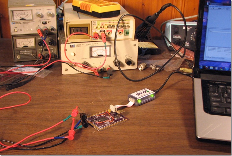
The A3PN250 board on the bench


I follow a few rules of thumb when smoke testing. These aren’t things one learns in books, but instead from other engineers, so they are worth writing down and passing on. Continue reading “Smoke testing the A3PN250 FPGA board”
SiliconBlue ultra-low-power FPGAs

Some time ago, I wrote, “The Actel/Microsemi parts have one additional advantage: They have the best static power consumption in the industry.”  I was wrong.

Last month, a post on the geda-user mailing list alerted me to SiliconBlue Technologies and their line of ultra-low-power FPGAs. These FPGAs are RAM-based, like those of the big two FPGA manufacturers, Xlinix and Altera. Unlike the chips from the big guys, though, SiliconBlue’s parts are not power hogs. In fact, they are fully static and go down to microamps with a static clock.  With the Microsemi (Actel) FPGAs, one has to freeze the FPGA with the “Flash Freeze” feature to get down to that level, but it appears that the SiliconBlue units simply clock right down there.  If true, that would give them quite an edge in power-conscious design.

Making a direct comparison between the Actel/Microsemi Igloo line, their lowest-powered, and the SiliconBlue parts has to be done on a case-by-case basis. The clock rates, and in particular, how often the clocks can be stopped, matter a lot. There is also the external configuration EEPROM for the Silicon Blue parts, which will take power in simple designs, but can be powered down or perhaps eliminated in more sophisticated uses.

In any event, I will stick with the Microsemi ProASIC3 and Igloo line for now. I like the convenience of a flash-based architecture. The next time I’m designing for low power, though,  it will be time to give SiliconBlue a good look.

Updated 5/12/11: The date of the geda-user post was corrected.

Making progress on the A3PN250 FPGA breakout…

I’ve made lots of small steps on the A3PN250 FPGA breakout board the last two weeks.

Firstly, I built an JTAG adapter cable to work around a wiring error on the PCB. When I laid out the board, I accidentally numbered the pins on the JTAG connector DIP-style instead of ribbon cable style.  That meant that all the pins except for pin 1 were wired wrong. After thinking a bit about the options, which included scrapping the board and starting over, or skywiring in corrected wiring for the connector, I decided the cleanest solution was to make a custom JTAG cable that moved the pins around where they belong. I’d seen other cables built this way. I asked myself, “How hard could it be?” Continue reading “Making progress on the A3PN250 FPGA breakout…”

Building the ProASIC 3 nano FPGA board

After a busy week spent traveling for work and a morning digging out from a surprise snowstorm, I had a great weekend with my family. It was Sunday night before I heated up the soldering iron and got down to business building the ProASIC 3 nano FPGA board.

I started with the toughest component, the FPGA. Its central location and low height means ….

After a busy week spent traveling for work and a morning digging out from a surprise snowstorm, I had a great weekend with my family.  It was Sunday night before I heated up the soldering iron and got down to business building the ProASIC 3 nano FPGA board.

I started with the toughest component, the FPGA.  Its central location and low height means that I will have an easier time accessing it before other components are mounted.  That is not likely to be a big problem for this board, with plenty of space around the chip, but I would still prefer not to have to work around the filter capacitors if I can avoid it.  On the other hand, its 100 pins and 0.5 mm pin pitch makes it far and away the most difficult soldering job on the PCB.

Continue reading “Building the ProASIC 3 nano FPGA board”

The FPGA boards are here… and they’re purple!

Despite my last post mentioning the lateness of the breakout boards, it turns out they had already arrived.  The mailer was stuck between two magazines in the mail, so my wife and I missed seeing it.  I had hoped to get the PCBs by February 26.  They were here the 22nd.  Oops!

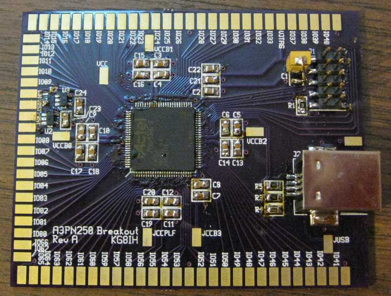
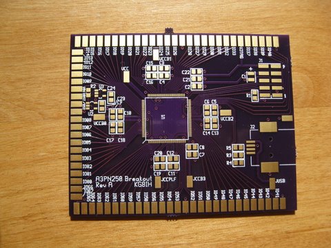
They came out quite nicely, with no obvious defects, and they look quite regal with gold plating and Laen’s signature purple solder mask. How often do you see purple circuit boards?  The gold is nice, too. Laen’s standard boards are have a solder finish, but sometimes some of his customers pay the extra for gold, in which case all the boards on that order come back with gold.

The FPGA board, gleaming and ready for some solder.

I’m looking forward to building up these boards and writing some Verilog to bring them to life.

No PCBs this week

I had hoped to be able to write about the new printed circuit boards this weekend, and maybe even show one built up, but they didn’t arrive. I had guessed that it would take them 9 days to get to Ohio from Oregon, which would have made them arrive yesterday.  There have been several snowstorms in areas they would be passing through, so it’s quite possible they were delayed by weather.

I’m still working on getting the Actel Microsemi development environment set up at home. When I tried to register for a free license key, the web site was down for maintenance.  I’m looking forward to getting it installed and starting work on some Verilog code. First up will be an iambic keyer.