gedasymbols.org is a great part of using gEDA

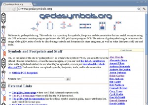
I’ve joined up as a contributor to  gedasymbols.org. This great resource, run by DJ Delorie, hosts schematic symbols for gschem and footprints for gEDA’s layout software, PCB. A search engine helps locate symbols and footprints, and gedasymbols includes links to other libraries off-site, such as Dan Luciani’s extensive footprint library. Gedasymbols.org has been hugely useful every time I do a design in gschem or PCB, and I’m happy to have something I can contribute back.

Gedasymbols has the symbols and footprints for the A3PN250 FPGA and AK5388 audio ADC breakout boards, plus symbols from an MSP430 project that I haven’t posted here yet.

As for other hacking recently, I’ve done parts placement for the AK5388 board but haven’t started routing it. I also need to make a better feedthrough panel for my antenna. I’ll have more to say about those two projects in a future post.

Comments welcome!
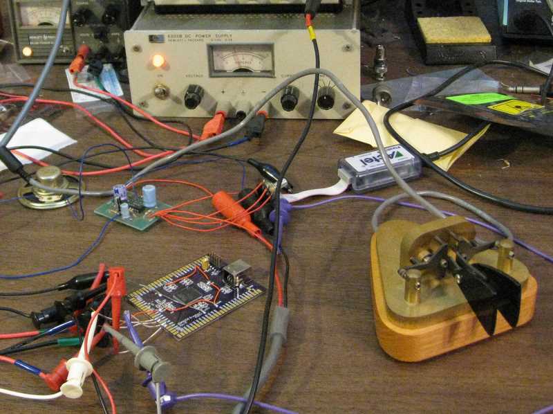
The iambic keyer core is alive

With just a few tweaks, I brought up the “IambicV” iambic keyer core on one of my A3PN250 breakout boards. I was stunned when it made dits, dahs, and iambic dah-dits perfectly the first time out. Yes, I know that’s what a testbench is supposed to make possible, and yes, I’ve had it happen before, but I still always expect smoke the first time I turn something on.

I made a few changes from last week’s version.

With just a few tweaks, I brought up the “IambicV” iambic keyer core on one of my A3PN250 breakout boards. I was stunned when it made dits, dahs, and iambic dah-dits perfectly the first time out. Yes, I know that’s what a testbench is supposed to make possible, and yes, I’ve had it happen before, but I still always expect smoke the first time I turn something on.

I made a few changes from last week’s version. One change was to invert the dit and dah pins. Although high-true logic is convenient within the keyer module, it seems like a good idea to have the actual paddles grounded, so the inputs had to be low-true. The physical constraints file enables the built-in pull-up resistors on the dit and dah pins.

For an audio amplifier, I used an old Saint Louis QRP Society LM380 board.

It’s all lashed together on my bench, but it works.

To download the core, see the iambic keyer project page.

Smoke testing the A3PN250 FPGA board

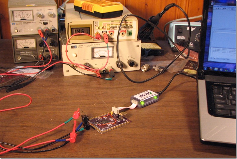
There comes a point in any project when one has to find out if it works, but first, there is the “smoke test”: Turn on the power and see if anything goes up in smoke. I smoke tested the A3PN250 FPGA breakout board this weekend, and it passed, or at least it failed to emit smoke. In any event, no smoke was emitted and the board survived. In fact, the board works. I talked to the board with a FlashPro4 programming pod and my rewired JTAG cable. The FPGA passed the pod’s signal-integrity check and identified itself correctly, so it is certainly alive.

The A3PN250 board on the bench


I follow a few rules of thumb when smoke testing. These aren’t things one learns in books, but instead from other engineers, so they are worth writing down and passing on. Continue reading “Smoke testing the A3PN250 FPGA board”

Making progress on the A3PN250 FPGA breakout…

I’ve made lots of small steps on the A3PN250 FPGA breakout board the last two weeks.

Firstly, I built an JTAG adapter cable to work around a wiring error on the PCB. When I laid out the board, I accidentally numbered the pins on the JTAG connector DIP-style instead of ribbon cable style.  That meant that all the pins except for pin 1 were wired wrong. After thinking a bit about the options, which included scrapping the board and starting over, or skywiring in corrected wiring for the connector, I decided the cleanest solution was to make a custom JTAG cable that moved the pins around where they belong. I’d seen other cables built this way. I asked myself, “How hard could it be?” Continue reading “Making progress on the A3PN250 FPGA breakout…”

Building the ProASIC 3 nano FPGA board

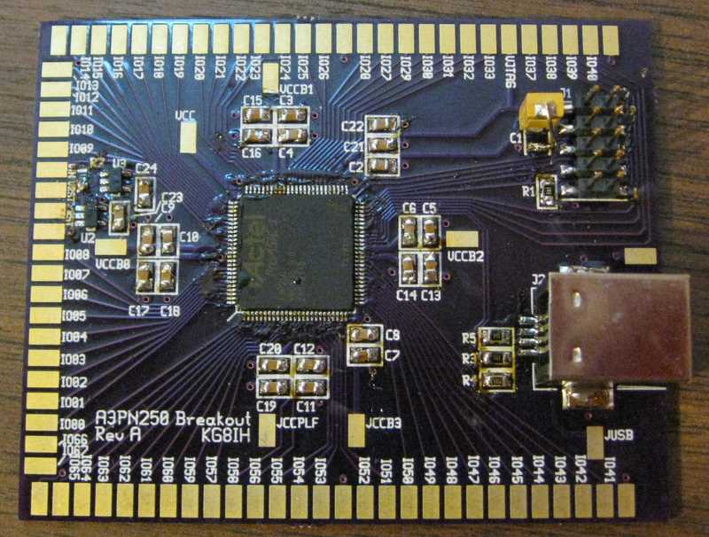
After a busy week spent traveling for work and a morning digging out from a surprise snowstorm, I had a great weekend with my family. It was Sunday night before I heated up the soldering iron and got down to business building the ProASIC 3 nano FPGA board.

I started with the toughest component, the FPGA. Its central location and low height means ….

After a busy week spent traveling for work and a morning digging out from a surprise snowstorm, I had a great weekend with my family.  It was Sunday night before I heated up the soldering iron and got down to business building the ProASIC 3 nano FPGA board.

I started with the toughest component, the FPGA.  Its central location and low height means that I will have an easier time accessing it before other components are mounted.  That is not likely to be a big problem for this board, with plenty of space around the chip, but I would still prefer not to have to work around the filter capacitors if I can avoid it.  On the other hand, its 100 pins and 0.5 mm pin pitch makes it far and away the most difficult soldering job on the PCB.

Continue reading “Building the ProASIC 3 nano FPGA board”

FPGA Breakout Board Layout

Here at last is the printed circuit board layout for the FPGA breakout board. I’m planning a series of projects involving FPGA-based DSP for ham radio, and in order to build them, I need an FPGA and a PCB on which to mount it….

The goals for this layout constrained it to be a nearly single-sided layout, …

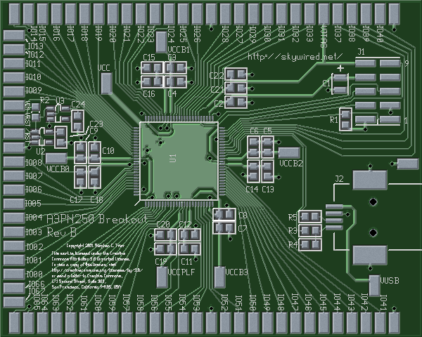
Here at last is the printed circuit board layout for the FPGA breakout board. I’m planning a series of projects involving FPGA-based DSP for ham radio, and in order to build them, I need an FPGA and a PCB on which to mount it. In the last installment of the project, I presented the schematic for the breakout board.

The goals for this layout constrained it to be a nearly single-sided layout, with a ground plane on the back. That way, the board could be mounted directly on a piece of copperclad with no short circuits to ground. My budget limited me to a double-sided board, so all signal and power traces had to go on the top side.

That said, here is the layout, top and bottom.

FPGA breakout PCB, top side

Continue reading “FPGA Breakout Board Layout”