Going Forth, or maybe not.

Over the years, I keep coming back to the Forth programming language. I admire its lean design and very efficient use of resources, but oh, is it ever quirky. My most recent return was motivated by James Bowman’s J1 Forth CPU, a small but blazingly fast FPGA-based processor.

My ambivalence with Forth started back in the 1980’s, when an engineer named Tom Harsch mentored a very young me in digital electronics and computer architecture. Tom is an all-around engineer, versed in both hardware and software. He had a fondness for Forth, and he introduced it to me. Or perhaps I should say

ME FORTH TOM INTRODUCED

You see, the very first quirk one runs into when encountering Forth is its use of postfix notation to represent operations. While mainstream languages like BASIC and C would have syntax resembling this,

print 2 + 3

Or this,

printf(“%d\n”, 2 + 3);

Forth, in common with German, likes its verbs last. Here’s the Forth version:

2 3 + .

Don’t overlook that period, “.”, at the end. In Forth, that does not end a sentence; it is the command for printing a number.

Postfix notation is intellectually appealing, for several reasons. In postfix, every operation can be expressed with the same basic syntax, so there is no longer a need to distinguish between infix operators (+, -, *, etc.), unary prefix operators (like negation, -), and function calls. They all fit the same basic syntactic framework. Another advantage is that it maps very simply onto a stack-based processor model, which in turn can be implemented reasonably efficiently on many traditional CPUs or which really flies on dedicated hardware.

Forth uses postfix notation to permit the implementation of a simple compiler, which is usually built right into the run-time environment. The simplicity of the compiler results in further bizarre constructs, like the IF…ELSE…THEN statement. Not only are “ELSE” and “THEN” ordered backwards from pretty much every other language in the world, thanks to postfix notation, the “THEN” keyword comes after the code for the ELSE:

( condition ) IF ( then-actions ) ELSE ( else-actions ) THEN

On the bright side, this did give rise to a classic bumper sticker from the Forth Interest Group:

FORTH LOVE IF HONK THEN

Defining a function is straightforward, if you don’t mind punctuation:

: 2times 2 * ;

The colon (:) command defines a new “word” for the language. The next text, “2times”, is the name of the new word. That is followed by the instructions for the word and a semicolon (;) that ends the definition.

So what does this new word do? It multiplies whatever number came before it by 2. “5 2times .” is equivalent to “5 2 * .” and prints the number 10.

This syntax is admirably compact and naturally lends itself to a functional style. On the other hand, what is the name of the word doing after the colon?  In a postfix language, I would expect to quote the name and the function body, then use the defining word. Something like this:

‘2times (2 *) :

Flip that around and add a “lambda” and it starts to look like LISP, but that’s a subject for another time. In Forth, this kind of quirkiness, where everything is postfix except for the parts that aren’t, is standard. It keeps Forth’s compiler simple, but at a cost in elegance.

Syntactic quirkiness aside, Forth has a  few things going for it. First, it makes extremely efficient use of machine resources. A reasonable Forth environment can fit in 4K of RAM and include a compiler, an interpreter, and room for a small application. A full-featured environment is larger, but still takes less resources than equivalent functionality in other languages. Forth is generally fairly speedy, too.

Forth is extremely versatile. The compiler is implemented in an extensible way. You can define Forth words that alter how the compiler works, giving another way to work at higher levels of abstraction.

The philosophy behind Forth encourages programs to be organized in a hierarchy of small, simple functions. Each layer of functions builds a higher level of abstraction than the one that lies below it. I like this kind of well-factored programming, and it would be nice to work in a language that encourages it.

That brings me to the J1 Forth CPU. This compact Verilog core is a work of brilliance, particularly in the way it uses the FPGA’s dual-port RAM in a carefully designed data path to achieve a high instruction rate. The instruction set architecture is pretty much pure Forth, and the implementation was written to be fast. James Bowman’s paper on the J1 (pdf) is well worth a read, and so is the Verilog source code.

Ever since I read the J1 paper, I’ve been itching to find a use for it. (Yes, I know, that’s a solution in search of a problem…) My oft-delayed R2/T2 transceiver project offered a chance. As I thought about what to put on the front panel, my mind strayed to thoughts of touch-panel LCDs. Wouldn’t it be nice to be able to defer most of the user interface decisions to software? It’s much easier to move a button on a screen than to un-drill a hole. eBay has a number of nice touch panels that would fit my chosen case perfectly.

Besides, I’ve been getting in a bit of a rut lately. Though there was a time when I learned every language I could find, lately I’ve been using C almost all the time. How better to shake things up than by implementing a touch-screen user interface in Forth?  My favorite way to learn a new language is to dive into a major project. In fact, I learned C by writing a text editor. Next I learned C++ by writing two text editors. Then I learned Tcl by writing a text editor, and Prolog by writing tax software. (Go figure.)

Eventually I came to my senses. First off, I’m so busy these days that I’m finding it hard to spend any time on the R2/T2, let alone write graphics software for it. A more serious problem, though, is that the Actel FPGA I have handy has only 6K of RAM and limited capability for ROM or flash. To do the graphical user interface, I would want fonts in two sizes, and the J1 on this FPGA would not be able to store even one. I was brainstorming ways to extend the J1’s address space into off-FPGA storage when I had my Arduino epiphany. It does not make sense to spend time engineering complex font storage when a cheap, off-the-shelf processor has 32K of flash and the gcc C compiler at the ready.

Even with the Arduino standing by, I can’t get avoid being busy. No, the R2/T2 will have to make do with switches and knobs. Maybe in the future I can replace them with a touchscreen.

That settled, only one problem remains: I no longer have a problem for the J1 and Forth to solve.

Oh, well…

Updated 1/18/13 to correct the IF…ELSE…THEN syntax.
Humbled by a sine wave oscillator

The old saw goes, “oscillators don’t, amplifiers do”, but that’s an analog saying.  It doesn’t apply to the digital world.  After all, digital is easy, while analog is hard, right?  (Be careful not to answer too quickly!)

For the last few weeks, I’ve spent my tinkering time on adding sine wave sidetone to the Verilog iambic keyer. As you may recall, sidetone is audio feedback for the keying, in other words, audible Morse code.  My thinking was that while this would appear to be a side trip on the way to FPGA-DSP radio nirvana, it would actually be valuable.  My vision for the radio will require sine wave synthesis in a couple of places.  Also, to have sine wave sidetone, I will need a digital-to-analog converter (DAC), so why not put theory into practice and build a delta-sigma DAC?

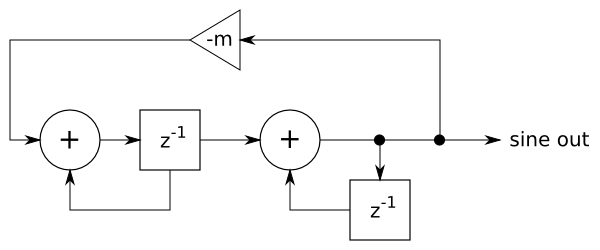
I looked around a bit to find a good way to synthesize a sine wave.  I didn’t want to do a simple ROM lookup table, because the radio will need memories for storing filter data and coefficients.  Instead, I settled on an algorithm that uses two integrators and a multiplier.  For some ratios of clock to output frequencies, the multiplication by -m can be reduced to a simple right-shift, which is always appealing to a hardware designer because it can be implemented without any gates.  The negation can then be absorbed into the first adder, costing little more than a set of inverters and a carry input.

Two-integrator sine wave oscillator

Then I found this elegant topology in Delta-Sigma Modulators: Modelling, Design, and Applications, by Bourdopoulos et al:

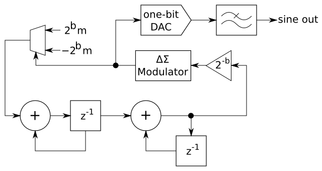
Digital sine wave oscillator with delta-sigma feedback

In this design, the multiplier has been replaced by a delta-sigma modulator and two constants.  This is gorgeous!  First of all, the multiplier is gone, replaced by a few adders and a mux.  Secondly, the delta-sigma bitstream is a built-in output for a DAC. There are a couple of wrinkles. First of all, there needs to be a scaling by 2^{-b} before and 2^b after the delta-sigma modulator. Otherwise, the modulator will see signals outside of its stable range. (Stability is a topic for a future tutorial in the How Delta-Sigma Works series.) Second, I’m not sure about putting the delay of the delta-sigma converter into the loop. It seems to me that the two integrators should be non-delaying. Third, are the two integrators sufficient filtering to remove the delta-sigma’s high-frequency noise, or is there a risk of high-frequency feedback making the loop unstable?

It sounds great, but when I coded it up in Verilog I couldn’t get it to be stable.  I fiddled with constants and bit widths for a while and couldn’t get it going. I also tried two non-delaying integrators in the loop. That didn’t work, either, and I couldn’t figure out why. Rather than do any stability analysis or model it in Octave, I decided to cut my losses and go to a more direct approach.

I took the original sine wave oscillator topology, which I easily got working, and tacked on a delta-sigma modulator to the output.  I decided to increase the clock rate in order to get a better signal-to-noise ratio (SNR) out of the DAC.  The oscillator blew up – unstable again!  After some more fiddling, I realized I was going to have to run with 24 or more bits of precision if I stuck to the design in the first figure.  To reduce the precision I needed to carry, I instead split the scaling between both integrators:

Sine wave oscillator followed by delta-sigma DAC

I fiddled with fewer bits, but with the clock-to-output frequency ratio I was working with (1 MHz clock, 800 Hz output), I needed all 16 bits to see a pretty sine wave in the ModelSim waveform viewer.

It looked great in the waveform viewer, so I burned it onto the FPGA and… noise. There is a brief tone buried in the noise, then it turns to all noise, and a little later, to a high-pitched whine without noise. The sine wave buried in the noise might mean I need better filtering between the FPGA and the audio amp (I didn’t use any, relying solely on the audio amp’s rolloff), but the all-noise and whining stages tell me that the oscillator or modulator is unstable. I probably didn’t run the testbench long enough in simulation to see it.

Meanwhile, at work, I’ve been having a great time introducing Test-Driven Development (TDD) into our firmware development process. The process was tedious at first, but now that I’ve been doing it long enough to see the results, I love it!  My code is better organized, better tested, and more solid than ever before.

That, combined with my frustration with the sine wave project, led me to think about applying Agile software engineering techniques to Verilog development.  I did some Google searches to see if anyone else is applying TDD or full Agile to hardware.  They are!  (agilesoc.com: Why Agile is a good fit for FPGA and ASIC development)

I learned some technical things while working on the sidetone. More importantly, though, I was reminded that methodical, well-tested development is not only better than seat-of-the-pants hacking, it is faster as well. Hobby projects benefit from discipline just as much as professional ones. I am going to set aside the sidetone project for a while and look at some other things.  Meanwhile I am going to think a bit about how to apply TDD and some other Agile concepts to my humble basement tinkering.

A Morse code keyer in VHDL

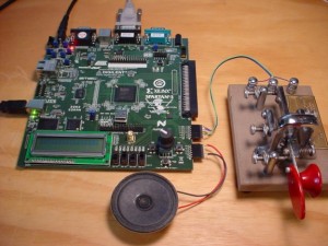
I found another FPGA Morse code keyer project! This one is written in VHDL by Jim Brady. He has posted the source (for a Xilinx Spartan 3A).  He also posted his vintage keyer designs from the 1960’s and 1970’s.

Jim’s design is not iambic, but does have dot and dash memory. Speed adjustment is done via an RS-232 serial link to a PC.

If VHDL is your hardware language of choice, or if just would like another take on Morse keying, Jim’s keyer is worth a look.  Of course, if you’re interested in a small iambic keyer core in Verilog, have a look at the skywired.net iambic keyer.

Update 8/8/11: Jim tipped me off to another VHDL keyer published online. This one is designed for a Cypress CPLD and is written in VHDL. It’s on pages 53-73 of Circuits I Have Known, by Ronald W. Parker. A PDF is available at controlsignalconverter.com, and the book itself is available at Amazon.

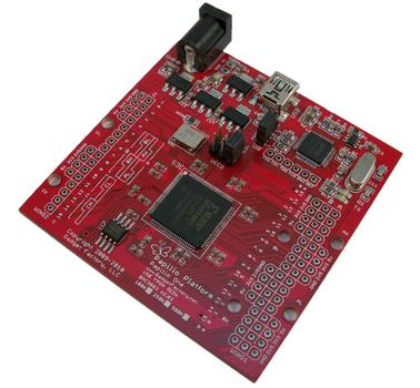
Papilio One Xilinx FPGA breakout board

This week, I came across the Papilio One FPGA board. This intriguing board mounts a Xilinx Spartan 3E, in either the 250K or 500K gate flavor, along with power supplies and an on-board USB programmer.  It’s inexpensive, at $50 for the 250K version and $70 for the 500K version. This would make a good pre-assembled alternative to the Microsemi SOC (née Actel) A3PN250 breakout board I am using.

One really neat feature of the Papilio is that it is designed to be Arduino-compatible! By loading an AVR8 soft core onto the FPGA, Arduino-compatible sketches can run on the board. The board supports a set of connectors to which up to 6 expansion boards (“wings”) can be attached, similar to shields. Its inclusion of a programmer and power supply also imitate the Arduino model.  As well as Arduino programs, the board is also programmable in Verilog and VHDL.

Unlike my board, its off-board connections are through-hole, and it can’t be mounted directly on a ground plane without extra insulation.  I like the philosophy of bringing out a full 48 uncommitted pins to the off-board connectors instead of loading up the board with extras.  Boards with RAMs, flash, and displays are easy to get started with, but end up being confining, making it harder to add external circuitry when the on-board stuff is not enough.

The Papilio is a close relative of the Open Bench Logic Sniffer, designed by Ian Lesnet and Jack Gassett. The Papilio heritage shows in the Logic Sniffer’s two “wing” expansion connectors.

If your FPGA preference is Xilinx or if you want a flexible, basic breakout board with an on-board programmer and power supply, the Papilio is well worth a look.

The iambic keyer core is alive

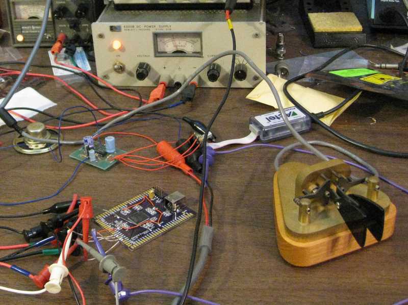
With just a few tweaks, I brought up the “IambicV” iambic keyer core on one of my A3PN250 breakout boards. I was stunned when it made dits, dahs, and iambic dah-dits perfectly the first time out. Yes, I know that’s what a testbench is supposed to make possible, and yes, I’ve had it happen before, but I still always expect smoke the first time I turn something on.

I made a few changes from last week’s version.

With just a few tweaks, I brought up the “IambicV” iambic keyer core on one of my A3PN250 breakout boards. I was stunned when it made dits, dahs, and iambic dah-dits perfectly the first time out. Yes, I know that’s what a testbench is supposed to make possible, and yes, I’ve had it happen before, but I still always expect smoke the first time I turn something on.

I made a few changes from last week’s version. One change was to invert the dit and dah pins. Although high-true logic is convenient within the keyer module, it seems like a good idea to have the actual paddles grounded, so the inputs had to be low-true. The physical constraints file enables the built-in pull-up resistors on the dit and dah pins.

For an audio amplifier, I used an old Saint Louis QRP Society LM380 board.

It’s all lashed together on my bench, but it works.

To download the core, see the iambic keyer project page.

Iambic keyer in Verilog

If my goal is to build an FPGA-based ham radio, one of the modules I can’t do without is an iambic keyer. I have to confess that I have never been much of a CW (Morse code) operator, but with so many logic gates available, it would be a shame to leave out a keyer.

Writing an iambic keyer turned out to be a good way to get the kinks out of the FPGA toolchain. The code itself is pretty simple and straightforward. One flip-flop keeps track of whether the current symbol is a dit or a dah. Another tracks whether the paddle for the opposite symbol (dah or dit, respectively) has been pressed during the current symbol. Finally, a two-level counter handles the timing of the dits and dahs and operates the key line. There is a simple sidetone, too.

If my goal is to build an FPGA-based ham radio, one of the modules I can’t do without is an iambic keyer. I have to confess that I have never been much of a CW (Morse code) operator, but with so many logic gates available, it would be a shame to leave out a keyer.

The basic idea behind an iambic keyer is to use a two-lever “paddle” to send Morse code. Pressing one paddle, usually with the thumb, sends a series of dits (dots), and pressing the other paddle, usually with the index finger, sends dahs (dashes). Squeezing both paddles alternates between dits and dahs. The didahdidahdidah… sound of squeezing the paddles sounds a bit like the iambic feet of English poetry, hence the name “iambic keyer”. If Shakespeare were a Morse code operator, one of his sonnets might include the sweet iambic pentameter “didahdidahdidah, didah didah!”

Writing an iambic keyer turned out to be a good way to get the kinks out of the FPGA toolchain. The code itself is pretty simple and straightforward. One flip-flop keeps track of whether the current symbol is a dit or a dah. Another tracks whether the paddle for the opposite symbol (dah or dit, respectively) has been pressed during the current symbol. Finally, a two-level counter handles the timing of the dits and dahs and operates the key line. There is a simple sidetone, too. Continue reading “Iambic keyer in Verilog”

The FPGA level shifter: not entirely crazy!

Some months ago, I came across an Actel app note that advocated using FPGAs as level shifters. “What a crazy waste of computing power,” I thought to myself, “though I suppose they are just trying to sell the low-end ProASIC3 nano FPGAs.” With that, I set the thought aside.

Much later, I ran into a problem.

Some months ago, I came across an Actel app note that advocated using FPGAs as level shifters. “What a crazy waste of computing power,” I thought to myself, “though I suppose they are just trying to sell the low-end ProASIC3 nano FPGAs.”  With that, I set the thought aside.

Much later, I ran into a problem. I had a prototype board to design. It had to plug into an existing, quite complicated microprocessor evaluation kit, adding a data radio and a few other functions to the system. After poring over the schematic for hours, the software developer, who I’ll call S, and I still weren’t 100% sure which pins on the expansion bus were free for our use, though we had a long list of pins that definitely were not suitable. On top of that, I had a level-shifting problem. The evaluation kit ran at 1.8 V and 2.75 V, with signals at both levels on the bus, but the radio required 3.3 V logic levels. Continue reading “The FPGA level shifter: not entirely crazy!”